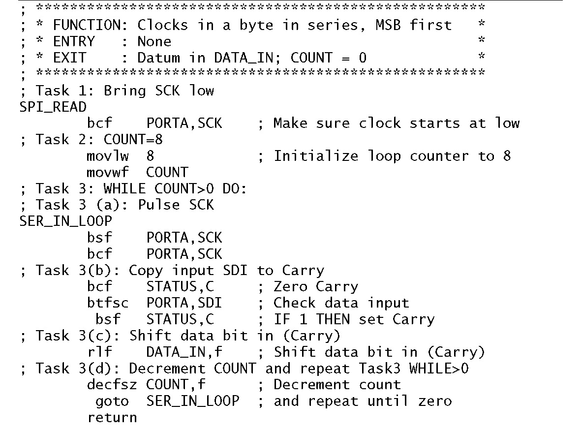
This task list is similar to that for subroutine SPI_WRITE except that the Carry bit is shifted into the file register, its value depending on the state of the SDI pin following the clock pulse. After eight clock-shift-test loops the datum in DATA_IN is the parallelized byte assembled from the serial input port, with the first bit ending up in the leftmost significant placeholder in DATA_IN.
Program 12.2 Input serial byte subroutine.
The subroutine coded in Program 12.2 is similar to the input subroutine of Program 12.1. Indeed they may be combined so that data is shifted out of a specified file register at at the same time as it is read in. This type of scheme is referred to as full duplex, as opposed to half duplex where only one direction at a time is possible. A serial link where data flow can only be in one fixed direction is known as simplex.
The serial protocol described in this example is commonly known as Serial Peripheral Interface (SPI).2 Microwire is a similar, but not identical, serial protocol.3 It is a sufficiently standardized protocol used by most microcontrollers to allow manufacturers to produce a range of peripheral devices specifically designed to directly interface to a SPI bus without the necessity to add external shift registers. As an example of this genre, the Maxim MAX549A is a dual digital to analog converter (DAC) which is powered with a VDD of +2.5 V to 5.5 V. Its operating current is typically 150 uA per DAC at 5 V and either or both DACs can be shut down to reduce the current drain to less than 1 us in its Standby mode. Data can be clocked in at a rate of up to 12.5 MHz.
A simplified functional diagram of the MAX549A is shown in Fig. 12.6. This shows an integral 16-stage shift register clocked from SCLK and fed data via DIN using the normal SPI protocol. The additional eight locations are used to store four control bits with the following functionality:
Enables the input PIPO register for channel A and which is clocked on a rising edge at the![]() pin.
pin.
Enables the input PIPO register for channel B and which is clocked on a rising edge at the![]() pin.
pin.
Gates both DAC registers allowing them to be simultaneously updated by a![]()
When 1 will power down any DAC selected with A0 or/and A1. This disconnects the reference voltage Vref from the DAC’s resistor network and leaves only the residual current of less than 1 uA to activate the internal registers whose contents remain unchanged.
Both DACs have a 2-layer register pipeline isolating them from the shift registers. The first layer is the In registers, which are gated when A0 or A1 as appropriate is 1. The data sitting in the lower byte of the shift register can then be clocked in by pulsing CE (pin 3) low. This change will 2SPI is a trademark of Motorola Inc.
3Microwire is a trademark of National Semiconductor Corp.be stored but will not appear at the input of the DAC until the next layer PIPO register is clocked. This register is enabled when C1 is 1 and![]() is pulsed. This means that one data byte can be sent to, say, DACA and then another to DACB. The DAC registers can then be updated together, resulting in both outputs VoutA and VoutB changing simultaneously; see Program 12.3. This can even be done when the MAX549A is asleep, as the registers are not affected by this power-down state.
is pulsed. This means that one data byte can be sent to, say, DACA and then another to DACB. The DAC registers can then be updated together, resulting in both outputs VoutA and VoutB changing simultaneously; see Program 12.3. This can even be done when the MAX549A is asleep, as the registers are not affected by this power-down state.
Fig. 12.6 The MAX549A SPI dual 8-bit DAC.
From this discussion we see that each transition from the PIC takes two 8-bit transfers___followed by a![]() on the
on the![]() pin.The MAX549A SPI dual 8-bit DAC.
pin.The MAX549A SPI dual 8-bit DAC.
For our example we will send the contents of File 20h to Channel A and then the contents of File 21 h to ChannelB, at that point updating both
DAC registers and hence outputting the analog equivalent of File 20h to pin VoutA and File 21 h to pin VoutB. We assume that both AD0 and AD1 pins are connected to Ground.
Our implementation will involve the transmission of four bytes of information:
1. Control byte 1: XXX00X01
No power down, update Channel A, no output change.
2. Data byte 1: Contents of File 20h.
3. Control byte 2: XXX01X10
No power down, update ChannelB, both outputs change.
4. Data byte 2: Contents of File 21 h.
The hardware-software interaction is shown in Program 12.3. Four bytes are transmitted using subroutine![]() , with the MAX549A’s
, with the MAX549A’s![]() being pulsed
being pulsed![]() after each
after each![tmp9191_thumb[2] tmp9191_thumb[2]](http://what-when-how.com/wp-content/uploads/2011/06/tmp9191_thumb2_thumb.png) byte pair. The final process sets C1 high, which transfers both data bytes to the DAC registers at the same time updating the Channel B In register.
byte pair. The final process sets C1 high, which transfers both data bytes to the DAC registers at the same time updating the Channel B In register.
Program 12.3 Interacting with the MAX549A dual-channel SPI DAC.
Fig. 12.7 SPI waveforms for the MAX549A.
Looking at the three pins on the MAX549A would give a waveform similar to that of Fig. 12.7 for the transmission of the first![]() byte pair. During the transmission CE remains low with the data shifting into the MAX549A’s integral shift register. After the second byte, i.e. the 16th clock pulse, bringing CE high activates the selected internal registers, executing the instruction.
byte pair. During the transmission CE remains low with the data shifting into the MAX549A’s integral shift register. After the second byte, i.e. the 16th clock pulse, bringing CE high activates the selected internal registers, executing the instruction.
The diagram shows transitions on the DIN line from the PIC’s SDO pin, occurring sometime before the active rising edge on SCK. Sometime is a vague term, obviously it must occur no later than a minimum time before _/ and be held for a short time after. The MAX549A data sheet gives the minimum set-up time tDS of 30 ns and hold time tDH of 10 ns. Even at a PIC clock rate of 20 MHz an instruction cycle takes 200 ns, so timing will not be violated.
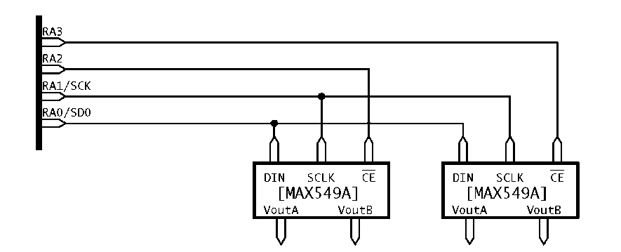
Fig. 12.8 Multiple MAX549As on the one SPI circuit.
By judicious use of the MAX549A’s CE input, several DACs maybe connected to the SCK/SD0 lines with a serial transmission only being shifted into the device which has its CE low. Figure 12.8 shows two MAX549As sharing the one SPI link, giving four analog output channels in total. Using a 2 to 4-line decoder in conjunction with RA3:2 would enable up to four MAX549As with a total budget of only four port lines.
All 28-pin+ mid-range and high-range PICs feature integral ports which can be configured to conform to several serial protocols. A somewhat simplified representation of the basic serial module, such as provided on the PIC16C73/4, set up for the SPI protocol is shown in Fig. 12.9. The heart of the Synchronous Serial Port (SSP) is the Special Purpose Register file (SPR) SSPBUF (SSP BUFfer) at File 13h. A datum byte written into this SPR will automatically be transferred into the SSP Shift Register (SSPSR) and shifted out of the PIC’s dedicated SD0 pin, which is shared with PortC’s RC5 I/O line. At the same time, eight bits of data will be shifted in from the SDI/RC4 pin. When this frantic burst of activity is completed, the new byte is automatically transferred to SSPBUF whence it can be read. This transfer is signalled by setting the BF (Buffer Full) flag in the SSPSTAT (SSP STATus) register at File94h – shown in Fig. 12.10. In addition, the SSP Interrupt flag SSPIF (Peripheral Interrupt Register 1 – see Fig. 14.10 ) is also set. Once SSPBUF is read, BF is automatically cleared. However, if using interrupts the SSPIF has to be ‘manually’ cleared in the ISR in the normal interrupt flag way.
The SSPSR can be clocked from four internal sources, which are selected by the programmer via the SSPMode bits SSPM[1:0] in the SSP CONtrol (SSPCON) register at File 14 h. Three of these frequencies are derived from the main PIC oscillator. For example, with a 20 MHz crystal the SCK/RC3 shift rate can be selected as 5, 1.25 MHz and 312.5 kHz (200, 800 ns and 3.2 us). The final selection gives the shift rate as half the frequency generated by Timer 2 overflowing – see Fig. 13.8. This option is used where very slow shift rates are required.
Fig. 12.9 The basic Serial Synchronous Port.
As well as programmable frequency selection the idle polarity of the SCK maybe set with the CKP bit at SSPCON[4]. With CKP = 0 the clock will idle low with valid data being made available on the ^ for an external shift register, as shown in Fig. 12.11.4
The two SSPMode combinations 0110k and 0101 b (see Table 12.1) place the SSP in the Slave mode. As opposed to the Master mode, shifting is done using an external clock, usually generated from a remote Master device. In addition, when in Slave mode 0100b the PIC can become a listener only if its SS (Slave Select) pin is high. This disconnects SDO and allows another Slave in a multidrop network to do the talking — see Fig. 12.12.
4A more advanced SSP port, such as used in the PIC16C774/F874, can control both active edge and idle polarity separately as well as input sampling time.
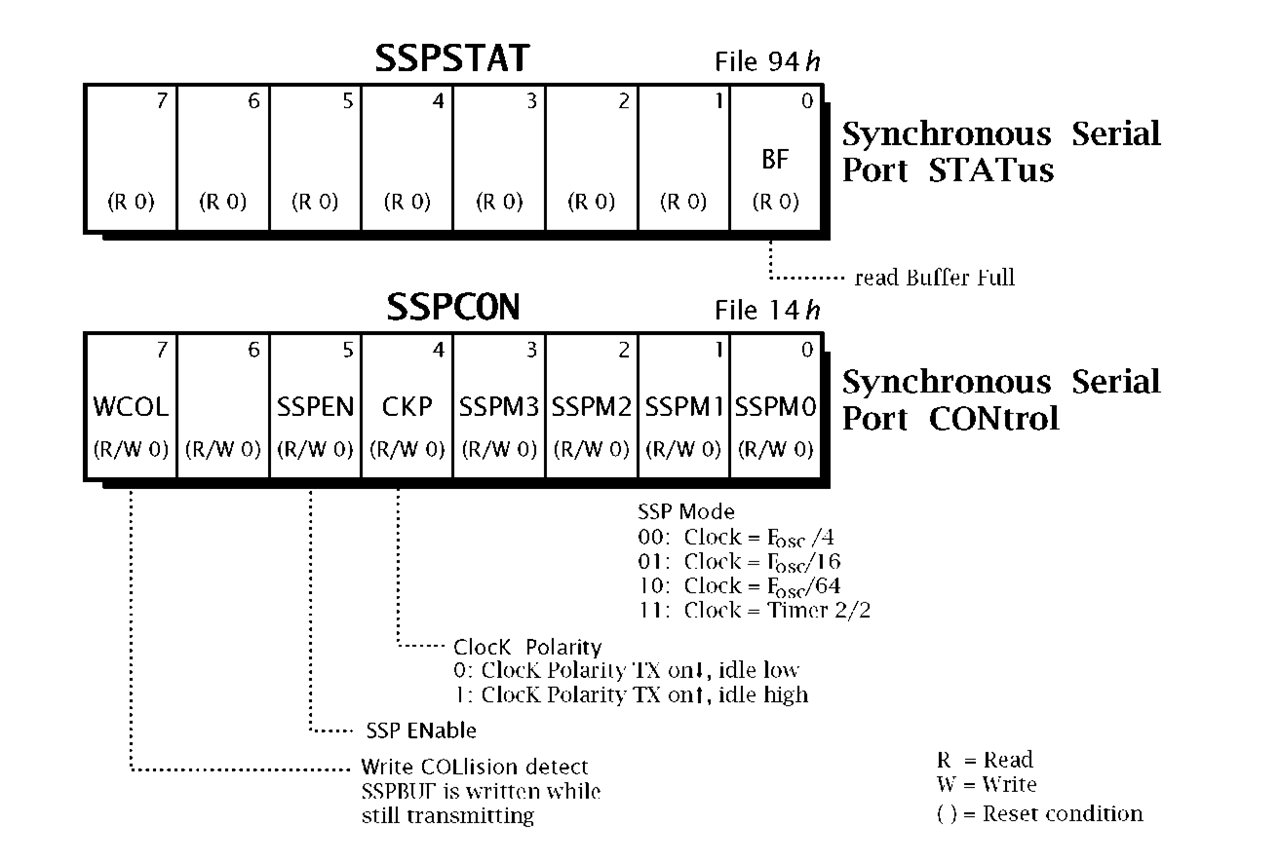
Fig. 12.10 The SSP Control and Status registers as appropriate to the SPI mode.
Figure 12.10 shows the SSP Control register at File 14h and the associated SSP Status register in Bank 1 at File 94h. The SSP port is enabled for whatever protocol when SSPEN (SSP ENable) in SSPCON[5] is 1. As SSPEN resets to zero, the SSP is disabled by default. In the disabled state the relevant PortC pins can be used as normal parallel I/O lines. If they are to be used as SSP lines then RC5:3 must be set via TRISC to be input or output as appropriate to their SSP function. Similarly, if the SS control is to be used, RA5 must be set to input.


