We have noted that digital processing is all about transmission, manipulation and storage of binary word patterns. Here we will extend the concepts introduced in the last topic as a lead into the architecture of the computer and microprocessor. We will look at some relevant logic functions, their commercial implementations and some practical considerations.
After reading this topic you will:
• Understand the properties and use of active pull-up, open-collector and 3-state output structures.
• Appreciate the logic structure and function of the natural decoder.
• See how a MSI implementation of an array of ENOR gates can compare two words for equality.
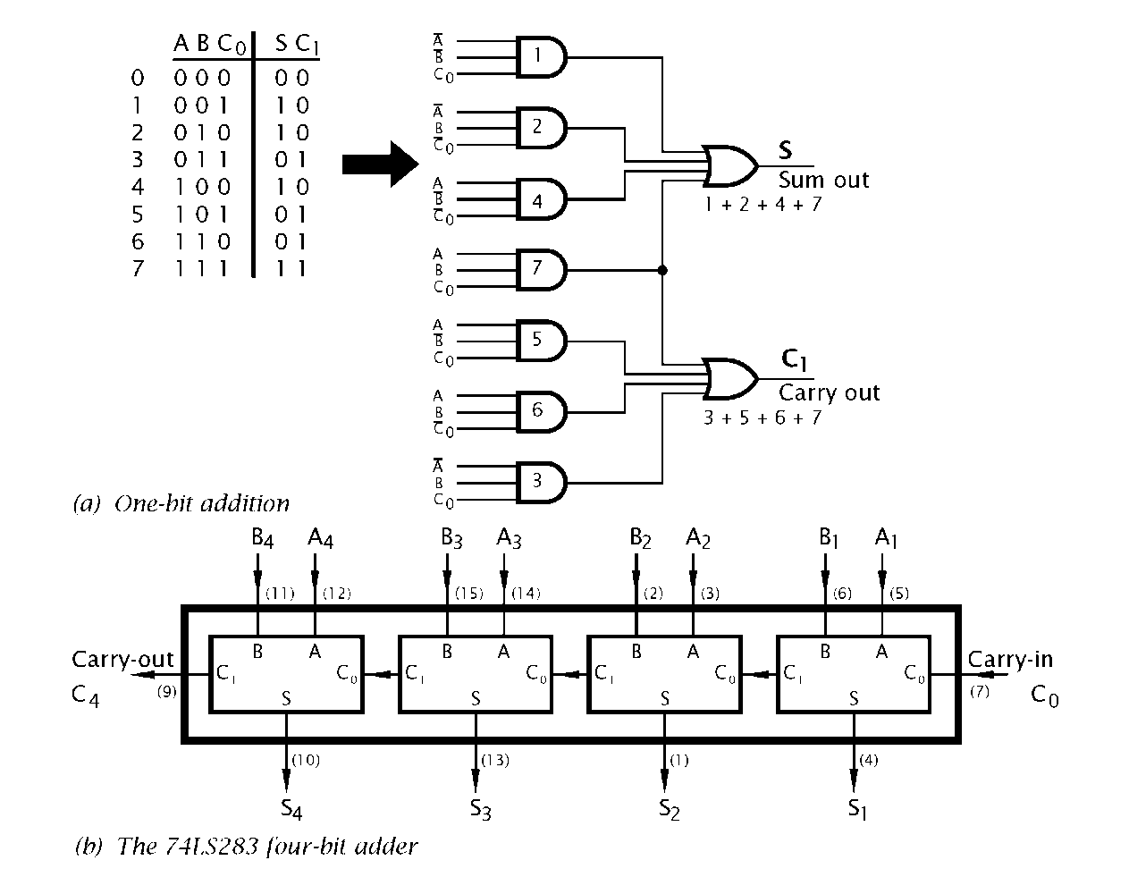
• Understand how a 1-bit adder can be constructed from gates, and can be extended to deal with the addition of two n-bit words.
• Appreciate how the function of an ALU is so important to a programmable system.
• Be aware of the structure and utility of a read-only memory (ROM).
• Understand how two cross-coupled gates can implement a R S latch.
• Appreciate the difference between a D latch and D flip flop.
• Understand how an array of D flip flops or latches can implement a register.
• See how a serial connection of D flip flops can perform a shifting function.
• Understand how a D flip flop can act as a frequency divide by two, and how a cascade of these can implement a binary count.
• See how an ALU/PIPO register can implement an accumulator processor unit.
• Appreciate the function of a RAM.
The first integrated circuits, available at the end of the 1960s, were mainly NAND, NOR and NOT gates. The most popular family of logic functions was, and still is, the 74 series transistor transistor logic (TTL); introduced by Texas Instruments and soon copied by all the major major semiconductor manufacturers.
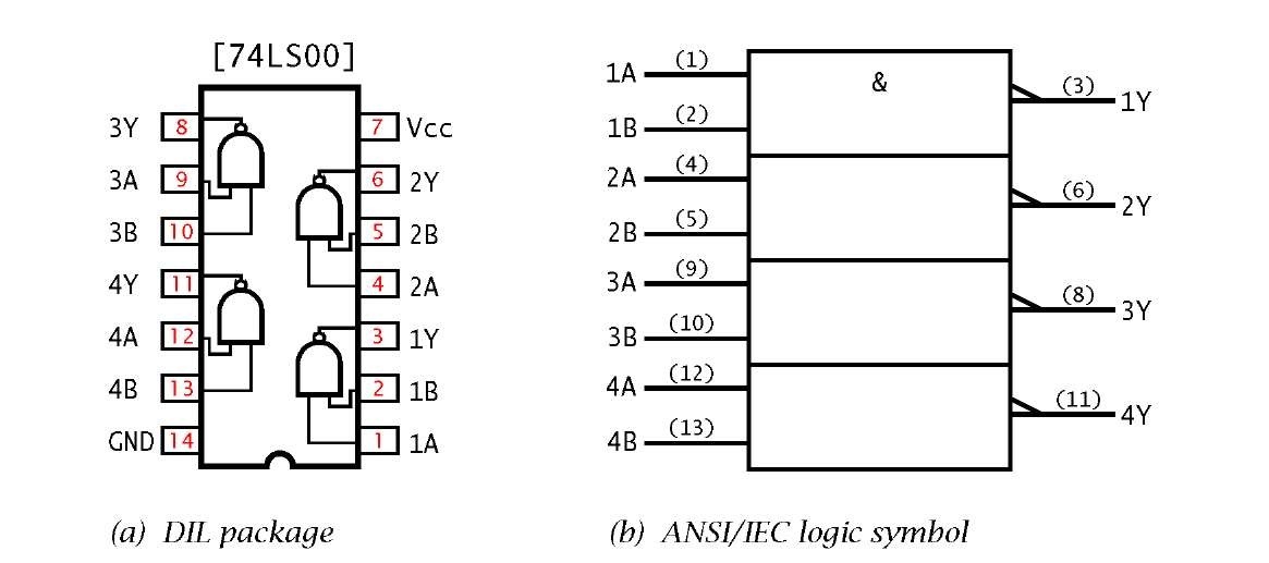
Fig. 2.1 The 74LS00 quad 2-I/P NAND package.
The 74LS001 comprises four 2-input NAND gates in a 14-pin package. The integrated circuit (IC) is powered with a 5 ± 0.25 V supply between VCC2 (usually about 5 V) and GND.The logic outputs are 2.4-5V High and 0-0.4V for Low. Most IC logic families require a 5V supply, but 3V versions are becoming available, and some CMOS implementations can operate with a range of supplies between 3 V and 15 V.
The 74LS00 IC is shown in Fig. 2.1(a) in its Dual In-Line (DIL) package. Strictly it should be described as a positive-logic quad 2-I/P NAND, as the electrical equivalent for the two logic levels 0 and 1 are Low (L is around ground potential) and High (H is around Vcc,3 usually about 5 V). If the relationship 0 — H; 1 — L is used (negative logic) then the 74LS00 is actually a quad 2-I/P NOR gate. The ANSI/IEC4 logic symbol of Fig. 2.1(b) denotes a Low electrical potential by using the polarity symbol. The ANSI/IEC NAND symbol shown is thus based on the real electrical operation of the circuit. In this case the logic coincides with a positive-logic NAND function. The & operator shown in the top block is assumed applicable to the three lower gates.
The output structure of a 74LS00 NAND gate is active pull-up. Here both the High and Low states are generated by connection via a low-resistance switch to Vcc or GND respectively. In Fig. 2.2(a) these switches are shown for simplicity as metallic contacts, but they are of course transistor derived.
Fig. 2.2 Output structures.
Logic circuits, such as the 74LS00, change output state in around 10 nanoseconds.5 To be able to do this, the capacitance of any interconnecting conductors and other logic circuits’ inputs must be rapidly discharged. Mainly for this reason, active pull-up (sometimes called totem-pole) outputs are used by most logic circuits. There are certain circumstances where alternative output structures have some advantages. The open-collector (or open-drain) configuration of Fig. 2.2(b) provides a ‘hard’ Low state, but the High state is in fact an open-circuit. The High-state voltage can be generated by connecting an external resistor to either Vcc or indeed to a different power rail. Non-orthodox devices, such as relays, lamps or light-emitting diodes, can replace this pull-up resistor. The output transistor is often rated with a higher than usual current and/or voltage rating for such purposes.
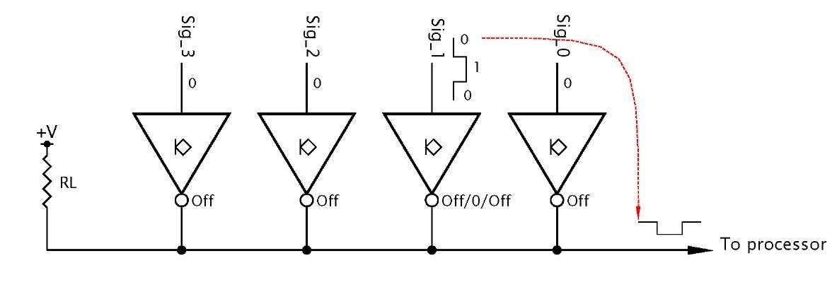
The application of most interest to us here is illustrated in Fig. 2.3. Here four open-collector gates share a single pull-up resistor. Note the use of the ^ symbol to denote an open-collector output. Assume that there are four peripheral devices, any of which may wish to attract the attention of the processor (eg. computer or microprocessor). If this processor has only one Attention pin, then the four Signal lines must be wire-ORed together as shown. With all Signals inactive (logic 0) the outputs of all buffer NOT gates are off (state H), and the party line is pulled up to +V by RL. If any Signal line is activated (logic 1), as in Sig_1, then the output of the corresponding buffer gate goes hard Low. This pulls the party line Low, irrespective of the state of the other signal lines, and thus interrupts the processor.
Fig. 2.3 Open-collector buffers driving a party line.
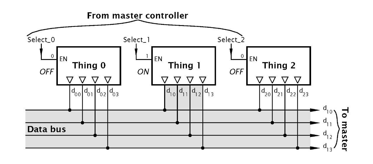
Fig. 2.4 Sharing a bus.
The three-state structure of Fig. 2.2(c) has the properties of both the preceeding output structures. When enabled, the two logic states are represented in the usual way by high and low voltages. When disabled, the output is open circuit irrespective of the activities of the internal logic circuitry and any change in input state. A logic output with this three-state is indicated by the V symbol.
As an example of the use of this structure, consider the situation depicted in Fig. 2.4. Here a master controller wishes to read one of several devices, all connected to this master over a set of party lines. As this data highway or Data bus is a common resource, so only the selected device can be allowed access to the bus at any one time. The access has to be withdrawn immediately the data has been read, so that another device can use the resource. As shown in the diagram, each Thing connected to the bus outputs, designated by the V symbol. When selected, only the active logic levels will drive the bus lines. The 74LS244 octal (x8) 3-state (sometimes called tri-state or TRIS) buffer has high-current outputs (designated by the t> symbol) specifically designed to charge/discharge the capacitance associated with long bus lines.
Integrated circuits with a complexity of up to 12 gates are categorised as Small-Scale Integration (SSI). Gate counts upwards to 100 on a single IC are Medium-Scale Integration (MSI), up to 1000 are known as Large-Scale Integration (LSI) and over this, Very Large-Scale Integration (VLSI). Memory chips and microprocessors are examples of this latter category.
Fig. 2.5 The 74LS138 and ’139 MSI natural decoders.
The NAND gate networks shown in Fig. 2.5 are typical MSI-complexity ICs. Remembering that the output of a NAND gate is logic 0 only when all its inputs are logic 1 then we see that for any combination of the Select inputs BA (21 20) in Fig. 2.5(a) only one gate will go to logic 0. Thus output Y2 will be activated when BA = 10. The associated truth table shows the circuit decodes the binary address BA so that address n selects output Yn. The 74LS139 is described as a dual 2 to 4-line natural decoder. Dual because there are two such circuits in the one chip. The symbol X/Y denotes converting code X (natural binary) to code Y (unary – one of n). The Enable input G is connected to all gates in parallel. Thus the decoder function only operates if G is Low (logic 0). If G is High, then irrespective of the state of BA (the X entries in the truth table denote a ‘don’t care’ situation) all outputs remain deselected – logic 1. An example of the use of the 74LS139 is given in Fig. 2.23.
The 74LS138 of Fig. 2.5(b) is similar, but implements a 3 to 8-line decoder function. The state of the three address lines CBA (22 21 20) n selects one only of the eight outputs Yn. The 74LS138 has three Gate inputs which generate an internal Enable signal G2B ■ G2A ■ G1. Only if both G2A and G2B are Low and G1 is High will the device be enabled.
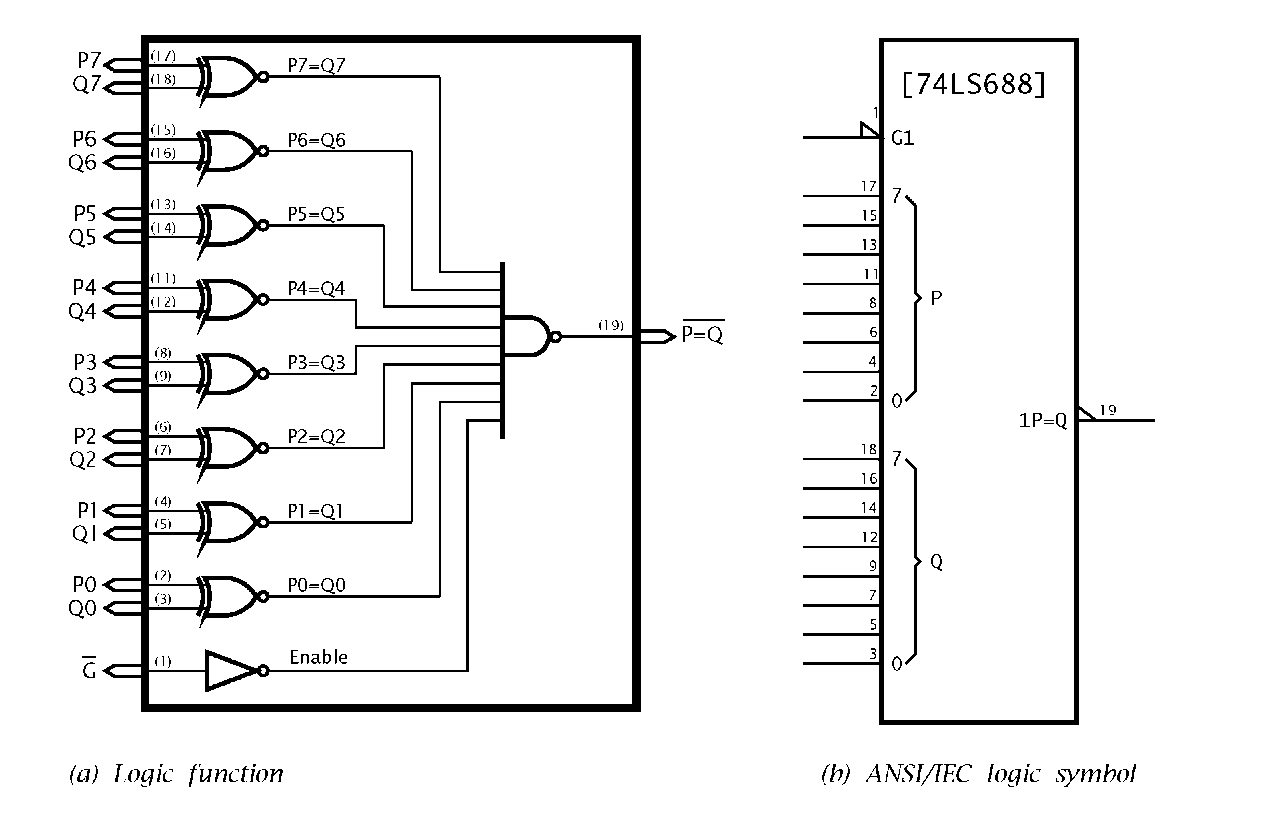
A large class of ICs implement arithmetic operations. The gate array illustrated in Fig. 2.6 detects when the 8-bit byte P7…P0 is identical to the byte Q7…Q0. Eight ENOR gates each give a logic 1 when its two input bits Pn, Qn are identical.Only if all eight bit pairs are the same, will the output NAND gate go Low. The 74LS688 Equality comparator also has a direct input G into this NAND gate, acting as an overall Enable signal.
The ANSI/IEC logic symbol, shown in Fig. 2.6(b) uses the COMP label to denote the arithmetic comparator function. The output is prefixed with the numeral 1, indicating that its operation P=Q is dependent on any input qualifying the same numeral; that is G1. Thus the active-Low Enable input G1 gates the active-Low output, 1P=Q.
One of the first functions beyond simple gates to be integrated into a single IC was that of addition. The truth table of Fig. 2.7(a) shows the Sum (S) and Carry-Out (C1) resulting from the addition of the two bits A and B and any Carry-In (C0). For instance row 6 states that adding two 1 s with a Carry-In of 0 gives a Sum of 0 and a Carry-Out of 1 (1 + 1 + 0 = 10). To implement this row we require to detect the pattern 110; that is A ■ B ■ Co; which is gate 6 in the logic diagram. Thus we have by ORing all applicable patterns together for each output:
Fig. 2.6 The 74LS688 octal equality detector.
Using such a circuit for each column of a binary addition, with the Carry-Out from column k -1 feeding the Carry-In of column k means that the addition of any two n-bit words can be simultaneously implemented. As shown in Fig. 2.7(b), the 74LS283 adds two 4-bit nybbles in 25 ns. In practice the final Carry-Out C4 is generated using additional circuitry to avoid the delays inherent on the carries rippling though each stage from the least to the most significant digit. n 74LS283s can be cascaded to implement addition for words of 4 x n width. Thus two 74LS283s perform a 16-bit addition in 45 ns; the extra time being accounted for by the carry propagation between the two units.
Adders can of course be coaxed into subtraction by inverting the minuend and adding one, that is 2′s complementation. An Adder/Subtractor circuit could be constructed by feeding the minuend word through an array of XOR gates acting as programmable inverters. The Mode line Add/Sub in Fig. 2.8 that controls these inverters also feeds the Carry-In, effectively adding one when in the Subtract mode.
Extending this line of argument leads to the Arithmetic Logic Unit (ALU). An ALU is a circuit which can undertake a selection of arithmetic and logic processes on input data as controlled by Mode inputs. The 74LS382 in Fig. 2.9 processes two 4-bit operands in eight ways, as controlled by the three Select bits S2 S1 S0 and tabulated in Fig. 2.9(a). Besides addition and subtraction, the logic operations of AND, OR and XOR are supported. The 74LS382 even generates the 2′s complement overflow function.
