There are many bistable implementations. For example, replacing the NOR gates by NAND gives a RS latch, where the inputs are active on a logic 0. The circuit illustrated in Fig. 2.14 shows such a latch used to de-bounce a mechanical switch. Manual switches are frequently used as inputs to logic circuits. However, most metallic contacts will bounce off the destination contact many times over a period of several tens of milliseconds before settling. For instance, using a mechanical switch to interrupt a computer/microprocessor will give entirely unpredictable results.
In Fig. 2.14, when the switch is moved up and hits the contact the latch is set. When the contact is broken, the latch remains unchanged, provided that the switch does not bounce all the way back to the lower contact. The state will remain Set no matter how many bounces occur. By symmetry, the latch will reset when the switch is moved to the bottom contact, and remain in this Reset state on subsequent bounces.
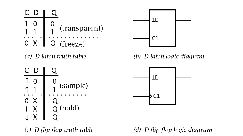
The D latch is an extension to the R S latch, where the output follows the D (Data) input when the C (Control) input is active (logic 1 in our example) and freezes when C is inactive. The D latch can be considered to be a 1-bit memory cell where the datum is retained at its value at the end of the sample pulse.
Fig. 2.15 The D latch and flip flop.
In Fig. 2.15(b) the dependency of the Data input with its Control is shown by the symbology C1 and 1D. The 1 prefix to D shows that it depends on any signal with a 1 suffix, in this case the C input. That is C1 clocks in the 1D data.
A flip flop is also a 1-bit memory cell, but the datum is only sampled on an edge of the control (known here as the Clock) input. The D flip flop described in Fig. 2.15(c) is triggered on a _/ (as illustrated in the truth table as t), but ^ clocked flip flops are common. The edge-triggered activity is denoted as > on a logic diagram, as shown in Fig. 2.15(d).
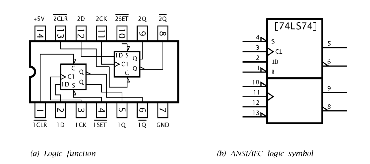
The 74LS74 shown in Fig. 2.16 has two D flip flops in the one SSI circuit. Each flip flop has an overriding Reset (R) and Set (S) input, which are asynchronous – that is not controlled by the Clock input. MSI functions include arrays of four, six and eight flip flops all sampling simultaneously with a common Clock input.
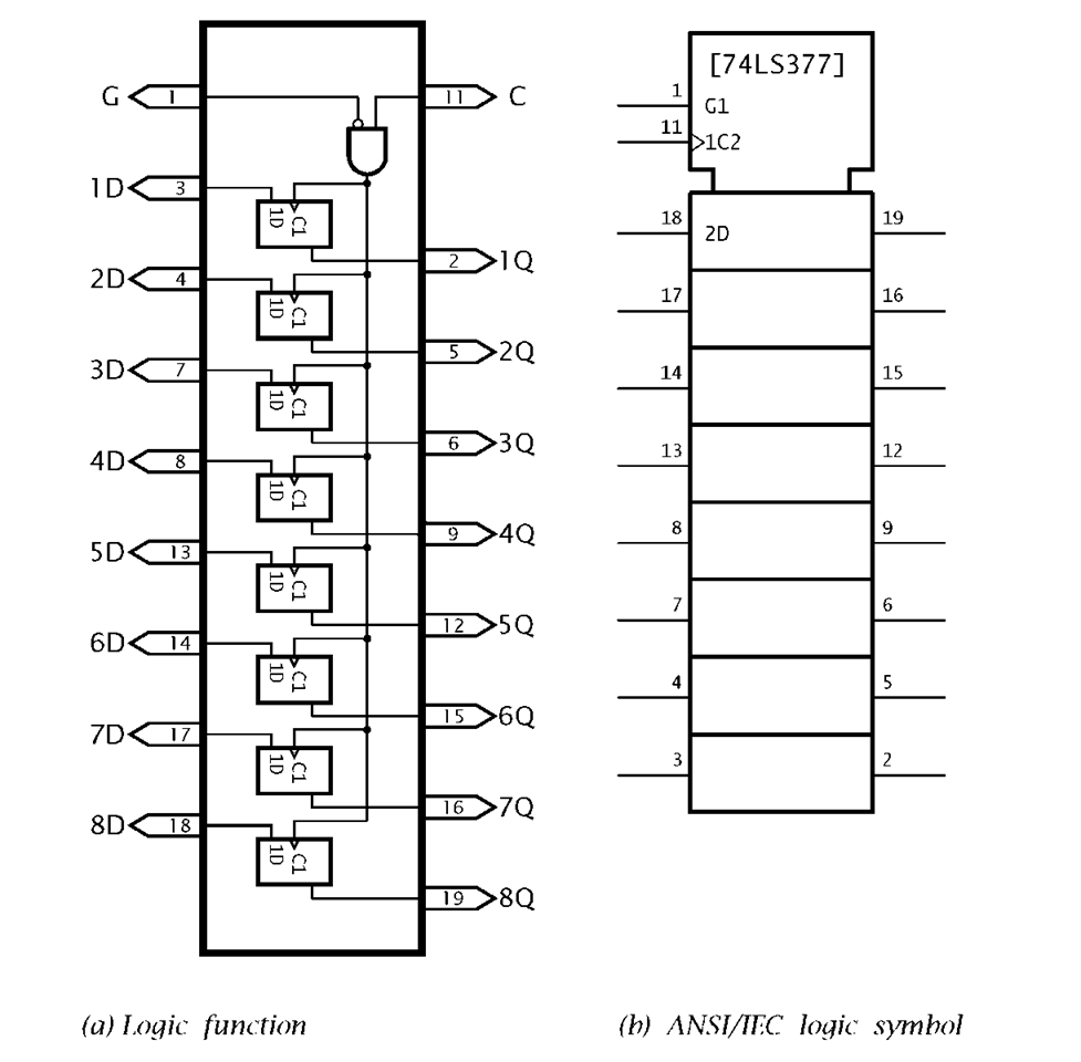
The 74LS377 shown in Fig. 2.17 consists of eight D flip flops all clocked by the same single Clock input C, which is gated by input G. Thus the 8-bit data 8D…1D is clocked in on the _/ of C if G is Low. In the ANSI/ISO logic diagram shown in Fig. 2.17(b), this dependency is indicated as G1^1C2^2D, which states that G enables the Clock input, which in turn acts on the Data inputs.
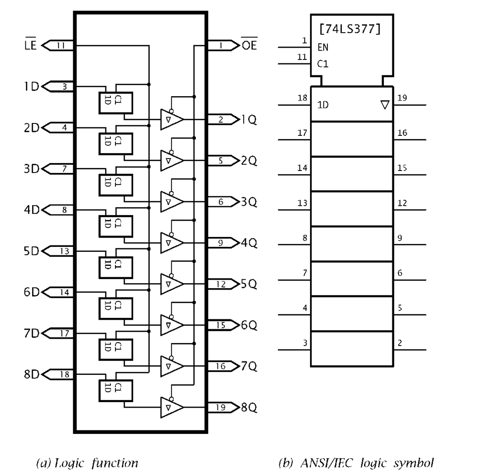
Arrays of D flip flops are known as registers; that is read/write memories that hold a single word. The 74LS377 is technically known as a parallel-in parallel-out (PIPO) register, as data is entered in parallel (that is all in one go) and is available to read at one go. D latch arrays are also available, such as the 74LS373 octal PIPO register shown in Fig. 2.18, in which the eight D flip flops are replaced by D latches. In addition the latch outputs have a 3-state capability. This is useful if data is to be captured and later put onto a common data bus to be read subsequently as desired by a computer.
Fig. 2.16 The 74LS74 dual D flip flop.
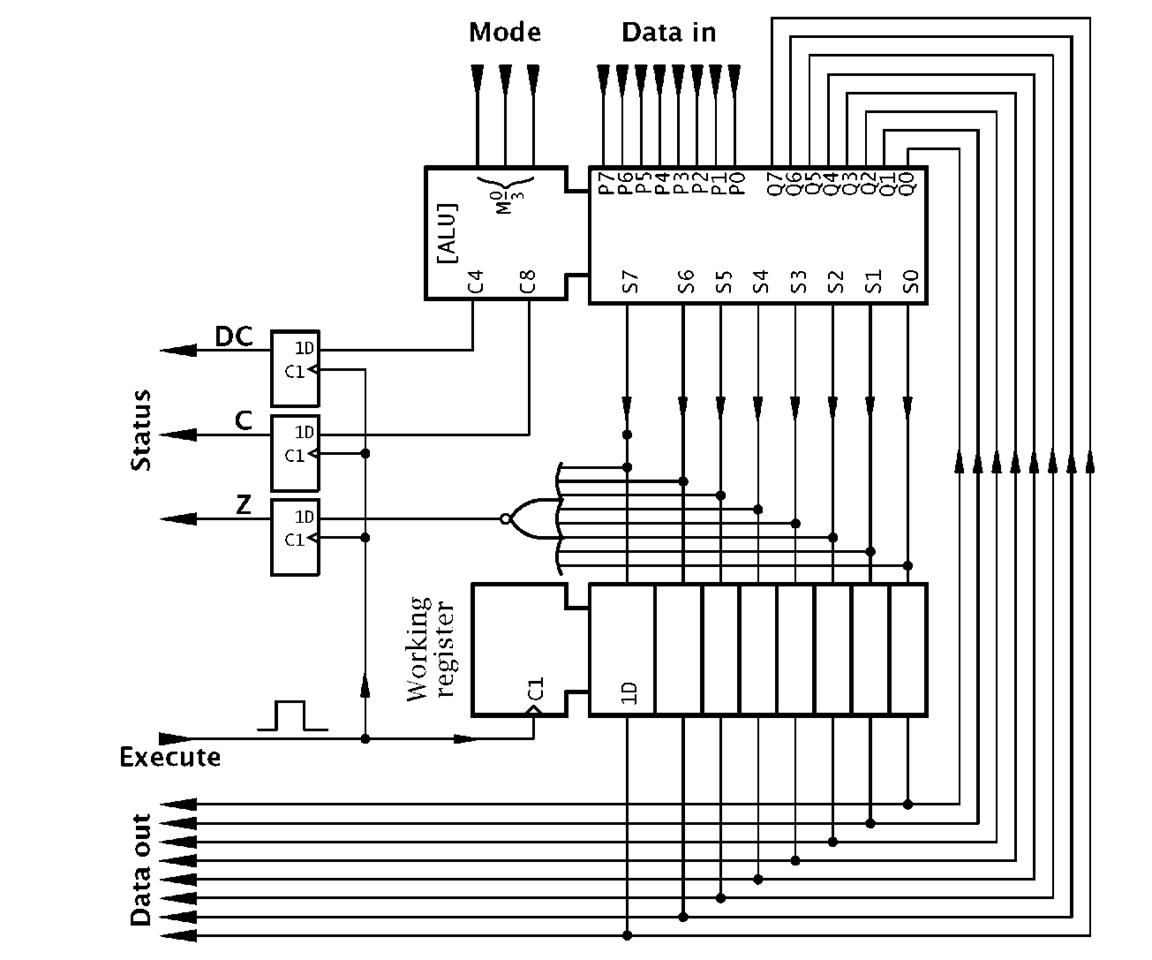
A pertinent example of the use of a PIPO register is shown in Fig. 2.19. Here an 8-bit ALU is coupled with an 8-bit PIPO register, accepting as its input the ALU output, and in turn feeding one input word back to the ALU. This register accumulates the outcome of a series of operations, and is sometimes called an Accumulator or Working register. To describe the operation of this circuit, consider the problem of adding two words A and B. The sequence of operations, assuming the ALU is implemented by cascading two 74LS382s might be:
Fig. 2.17 The 74LS377 octal D flip flop array.
• Data out is Word B plus Word A.
The sequence of operation codes, that is 000 – 100 – 100 constitutes the program. In practice each instruction would also contain the address (where relevant) in memory of the data to be processed; in this case the locations of Word A and Word B.
Each outcome of a process will have associated properties. For example it may be zero or have a carry-out. Such properties may be significant in the future progress of the program. In the diagram three D flip flops, clocked by Execute, are used to grab this status information. In this situation the flip flops are usually known as flags (or sometimes semaphores). Thus we have Z (Zero), C (Carry from bit 7) and DC (BCD Carry from bit 3) flags, which form a Code Condition or Status register.
Fig. 2.18 The 74LS373 octal D latch array.
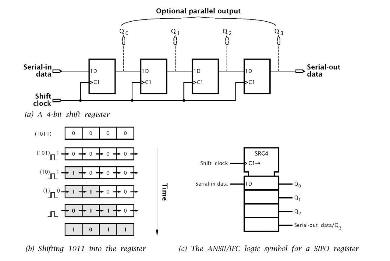
There are various other forms of register. The 4-bit shift register of Fig. 2.20(a) is an example of a serial-in serial-out (SISO) structure. In this instance the data held in the nth D flip flop is presented to the input of the (n + 1 )th stage. On receipt of a clock pulse (or shift pulse in this context), this data moves into this (n + 1)th flip flop, i.e. effectively moving from stage n to stage n + 1. As all flip flops are clocked simultaneously, the entire word moves once right on each shift pulse.
In the example of Fig. 2.20 a 4-bit external data nybble is fed into the left-most stage bit by bit as synchronised by the clock. After four shift pulses the serial 4-bit word is held in the register. To get it out again, four further shifts moves the wrod bit by bit out of the shift register, this is SISO. If the individual flip flops are accessible then the data can be accessed at one go, that is serial-in parallel-out.
Fig. 2.19 An 8-bit ALU-accumulator processor.
The logic diagram of Fig. 2.20(b) uses the — symbol affected by the clock input to indicate the shift action, C1 —. SRG4 indicates a Shift ReGister 4-stage architecture.
Other architectures include parallel-in serial-out which is useful for parallel to serial conversion. Counting registers (counters) increment or decrement on each clock pulse, according to a binary sequence. Typically an n-bit counter can perform a count of 2n states. Some can also be loaded in parallel and thus act as a store.
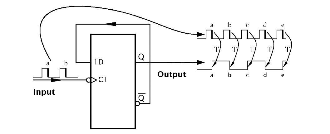
Consider the negative-edge triggered D flip flop shown in Fig. 2.21 where its Q output is connected back to the 1D input. On each ^ at the Clock input C1 the data at the 1D input will be latched in to appear at the Q output. As it is the complement of this output that is fed back to the input, then the next time the flip flop is clocked the opposite logic state will be latched in. This constant alternation is called toggling and is depicted on the diagram by T. The output waveform resulting from a constant frequency input pulse train is half this frequency. This waveform is a precision squarewave, provided that the input frequency remains constant. This T flip flop is sometimes known as a binary or a divide-by-2.
Fig. 2.20 The SISO shift register.
Fig. 2.21 The T flip flop.
