Both the examples involve adding an 8-bit to a 16-bit operand. Where the former is positive, the data may be increased to 16 bits by padding with 0s. The situation is slightly less intuitive where negative data requires extension. Here the prescription is to extend the data by padding out with 1 s. In the general case the rule is simply to pad out data by propagating the sign bit left. This technique is known as sign extension.
Multiplication by the nth power of two is simply implemented by shifting the data left n places. Thus 00101 (5) << 01010(10) << 10100(20) multiplies 5 by 22, where the << operator is used to denote shifting left. The process works for signed numbers as well:
Should the sign bit change polarity, then a magnitude bit has overflowed. Some computers/microprocessors have a Arithmetic Shift Left process that signals this situation, as opposed to the standard Logic Shift Left used in unsigned number shifts.
Multiplication by non-powers of 2 can be implemented by a combination of shifting and adding. Thus as shown in (c) above, 3 x 10 is implemented as (3 x 8) + (3 x 2) = (3 x 10) or (3 << 3) + (3 << 1).
In a similar fashion, division by powers of 2 is implemented by shifting rightnplaces. Thus 1100(12) >> 0110(6) >> 0011(3) >> 0001.1(1.5). This process also works for signed numbers:
Notice that rather than always shifting in 0s, the sign bit should be propagated in from the left. Thus positive numbers shift in 0s and negative numbers shift in 1 s. This is known as Arithmetic Shift Right as opposed to Logic Shift Right which always shifts in 0s.
Division by non powers of 2 is illustrated in (c) above. This shows the familiar long division process used in decimal division. This is an analagous process to the shift and add technique for multiplication, using a combination of shifting and subtracting.
Arithmetic is not the only way to manipulate binary patterns. George Boole8 in the mid-19th century developed an algebra dealing with symbolic processing of logic propositions. This Boolean algebra deals with variables which can be true or false. In the 1930s it was realised that this mathematical system could equally well be used to analyze switching networks and thus binary logic systems. Here we will confine ourselves to looking at the fundamental logic operations of this switching algebra.
 |
 |
|
(a) Truth table |
(b) Alternative logic symbols |
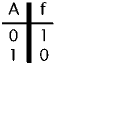
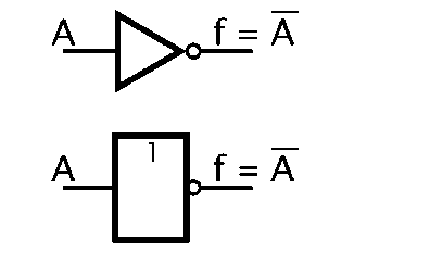
Fig. 1.1 The NOT operation.
The inversion or NOT operation is represented by overscoring. Thus f = A states that the variable f is the inverse of A; that is if A = 0 then f = 1 and if A = 1 then f = 0. In Fig. 1.1(a) this transfer characteristic is presented in the form of a truth table. By definition, inverting twice returns a variable to its original state; thus f = f .9
Logic function implementations are normally represented in an abstract manner rather than as a detailed circuit diagram. The NOT gate is symbolized as shown in Fig. 1.1(b). The circle always represents inversion in a logic diagram, and is often used in conjunction with other logic elements, such as in Fig. 1.2(c).
The AND operator gives an all or nothing function. The outcome will only be true when every one of the n inputs are true. In Fig. 1.2 two input variables are shown, and the output is symbolized as f = B ■ A, where is the Boolean AND operator. The number of inputs is not limited to two, and in general f = A(0) A(1) A(2) A(n). The AND operator is sometimes called a logic product, as ANDing (cf. multiplying) any bit with logic 0 always yields a 0 output.
If we consider B as a control input and A as a stream of data, then consideration of the truth table shows that the output follows the data stream when B = 1 and is always 0 when B = 0. Thus the circuit can be considered to be acting as a valve, gating the data through on command. The term gate is generally applied to any logic circuit implementing a fundamental Boolean operator.
Most practical AND gate implementations have an inverting output. The logic of such implementations is NOT AND, or NAND for short, and is symbolized as shown in Fig. 1.2(c).
Fig. 1.3 The inclusive-OR operation.
The inclusive-OR operator gives an anything function. Here the outcome is true when any input or inputs are true (hence the > 1 label in the logic symbol). In Fig. 1.3 two inputs are shown, but any number of variables may be ORed together. ORing is sometimes referred to as a logic sum, and the + used as the mathematical operator; thus f = B + A. In an analogous manner to the AND gate detecting all ones, the OR gate can be used to detect all zeroes.
Considering B as a control input and A as data (or vice versa), then from Fig. 1.3(a) we see that the data is gated through when B is 0 and inhibited (always 1 ) when B is 1 . This is a little like the inverse of the AND function. In fact the OR function can be expressed in terms of AND using the duality relationship A + B = B ■ A. This states that the NOR function can be implemented by inverting all inputs into an AND gate.
AND, OR and NOT are the three fundamental Boolean operators. There is one more operation commonly available as an electronic gate; the Exclusive-OR operator (XOR). The XOR function is true if only one input is true (hence the =1 label in the logic symbol). Unlike the inclusive-OR, the situation where both inputs are true gives a false outcome.
Fig. 1.4 The XOR operation.
If we consider B is a control input and A as data (they are fully interchangeable) then:
• When B = 0 then f = A; that is the output follows the data input.
• When B = 1 then f = A; that is the output is the inverse of the data input.
Thus an XOR gate can be used as a programmable inverter.
Another useful property considers the XOR function as a logic differentiator. The XOR truth table shows that the gate gives a true output if the two inputs differ. Alternatively, the ENOR truth table of Fig. 1.4(c) shows a true output when the two inputs are the same. Thus an ENOR gate can be considered to be a 1-bit equality detector. The equality of two n-bit words can be tested by ANDing an array of ENOR gates, each generating the function Bk ® Ak; that is:
As a simple example of the use of the XOR/XNOR gates, consider the problem of detecting sign overflow. This occurs if both the sign bits of word B and word A are the same![]() AND the sign bit of the outcome word C is not the same as either of these sign bits, say SB ® SC. The logic diagram for this detector is shown in Fig. 1.5 and implements the Boolean function:
AND the sign bit of the outcome word C is not the same as either of these sign bits, say SB ® SC. The logic diagram for this detector is shown in Fig. 1.5 and implements the Boolean function:
Fig. 1.5 Detecting sign overflow.
Finally, the XOR function can be considered as detecting when the number of true inputs are odd. By cascading n + 1 XOR gates, the overall parity function is true if the n-bit word has an odd number of ones. Some measure of error protection can be obtained by adding an additional bit to each word, so that overall the number of bits is odd. This oddness can be checked at the receiver and any deviation indicates corruption.
![tmp1853_thumb[2] tmp1853_thumb[2]](http://what-when-how.com/wp-content/uploads/2011/06/tmp1853_thumb2_thumb.jpg)
![tmp1854_thumb[2] tmp1854_thumb[2]](http://what-when-how.com/wp-content/uploads/2011/06/tmp1854_thumb2_thumb.jpg)


![tmp1860_thumb[2] tmp1860_thumb[2]](http://what-when-how.com/wp-content/uploads/2011/06/tmp1860_thumb2_thumb.jpg)

