Parallel data transmission is fast, with a minimum of software overhead. However, there are circumstances where its use is inappropriate; either because of the additional hardware cost or more commonly where the receivers are geographically distant, with the concomitant cost or non availability of multiple communication channels and their necessary interface hardware. In such situations data can be sent one bit at a time and assembled by the remote device into the original data bytes. In this manner a comparison can be made with the parallel port on a PC, commonly used for local peripherals, such as a printer, and the serial port frequently used with a modem to link into the internet via a single telephone line.
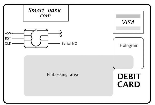
Fig. 12.1 The smart card.
As an example, consider the smart cards in your wallet. Each card will have an embedded microcontroller, typically 8-bit, giving it its intelligence. Cost constraints are severe to give a manufacturing price of under $1, and a large component of this is accounted by the non corrosive gold-plated contacts via which the microcontroller is powered and clocked when in contact with the card reader. In order to keep the mechanical precision of the reader low and hence reliability high, the number of contacts must be minimized and pad size maximized.
The standard arrangement shown in Fig. 12.1 uses contacts to provide the two power nodes, Reset, Clock and one line to allow data to be shifted in or out one bit at a time. Although this is relatively slow, in comparison to the human-mechanical constraints speed is not an issue. Furthermore, contact between the reader/automatic teller and the central computer, perhaps several thousands of miles/kilometers away, will typically be via a single channel telephone or ISDN line.
In this topic we will examine a range of techniques used to serially transmit data, both using bespoke shift register circuits and industrial devices using standard communication protocols. After reading this topic you will:
• Understand the need for serial transmission.
• Be able to design serial ports and associated software routines to communicate with standard parallel peripheral devices.
• Be capable of interfacing serial peripheral devices using both the SPI and I2C protocols.
• Appreciate the need for asynchronous serial communication and be able to write software drivers conforming to this protocol.
• Be able to use the integral Universal Synchronous Asynchronous Receiver/Transmitter Port (USART) for asynchronous protocols.
• Understand the necessity for buffering long distance communication circuits.
Examine the parallel 3-digit 7-segment display interface of Fig. 11.13 which uses both the parallel ports A and B. Although this is a working circuit, most of the parallel port budget of an 18-pin footprint device has been used up. Speed is certainly not a factor here, so a slower mode of data transmission is acceptable.
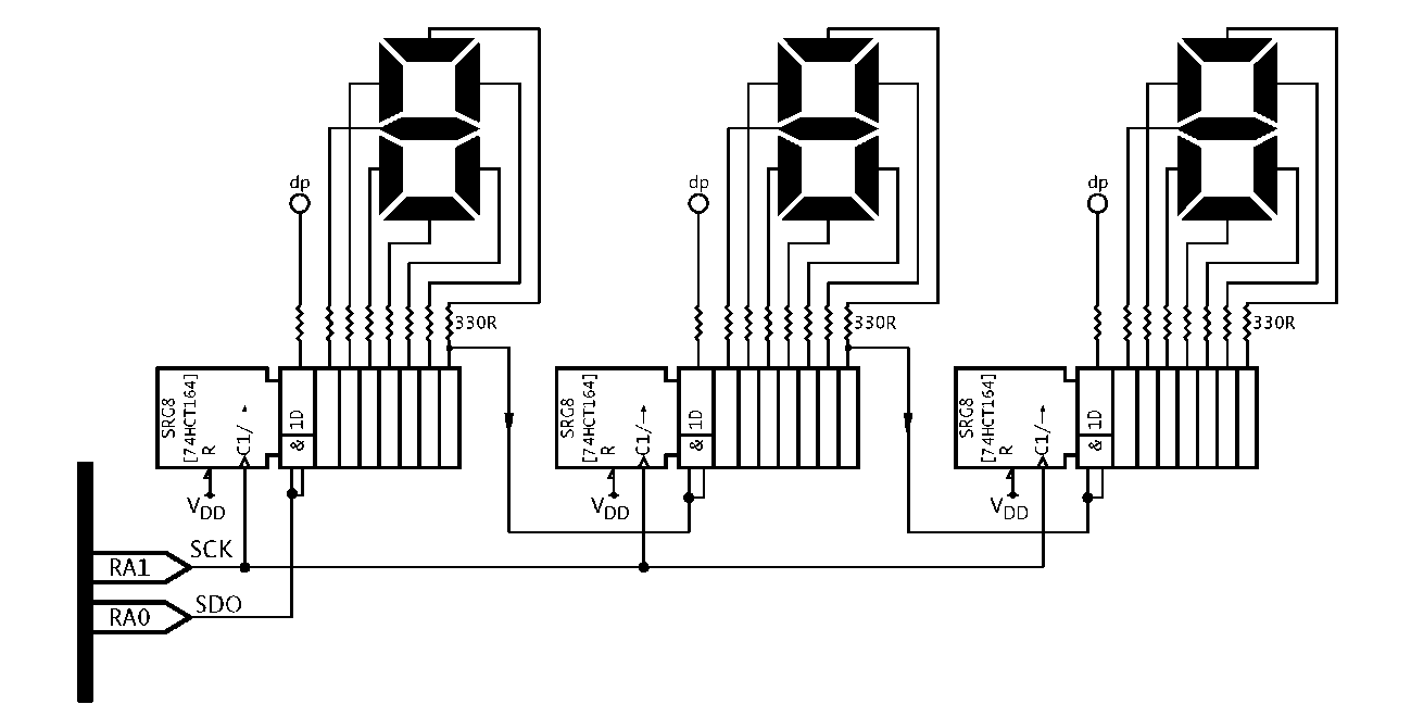
Consider the serial equivalent of Fig. 12.2. Here only two port pins are used. One labelled SDO (Serial Data Output) outputs the data bit by bit, most significant bit first. The other, labelled SCK (Serial ClocK) is used to clock the three shift registers at the one time, and hence shift the data right one bit at a time.
Each display has an associated 74HCT164 8-bit shift register1 – see Fig. 2.20.The 74HCT164 has a positive-edge triggered shift input clock C1 and two serial data inputs ANDed together at 1D. One of these data inputs can be used to gate the other input, but in our example they are both connected together to give a single serial input. There is also an active-low Reset input to clear the register contents, which are held high in the diagram. If desired, another port line can be used to drive R.
To change the display, a total of 24 bits will have to be shifted into the register array. To see how this can be done we will repeat the 7-segment driver routine of Program 11.7 which converts a binary byte to an array of BCD digits in HUNDREDS, TENS and UNITS. These are mapped to 7-segment code and then sent out to each digit 8-bits at a time.
1All data outputs are simultaneously available and thus the 74HCT164 is described as a Serial-In Parallel-Out (SIPO) register as well as a SISO shift register.
Fig. 12.2 Serial interface to a 3-digit 7-segment display.
To serialize this process we require to design a subroutine to put each bit of a specified file register DATA_OUT out at SDO while pulsing SCK, beginning with the leftmost bit. A task list for such a subroutine is:
1. Bring SCK low.
2. COUNT = 8.
3. WHILE COUNT > 0 DO:
(a) Shift DATA_OUT left into Carry.
(b) Copy Carry to SDO.
(d) Decrement COUNT.
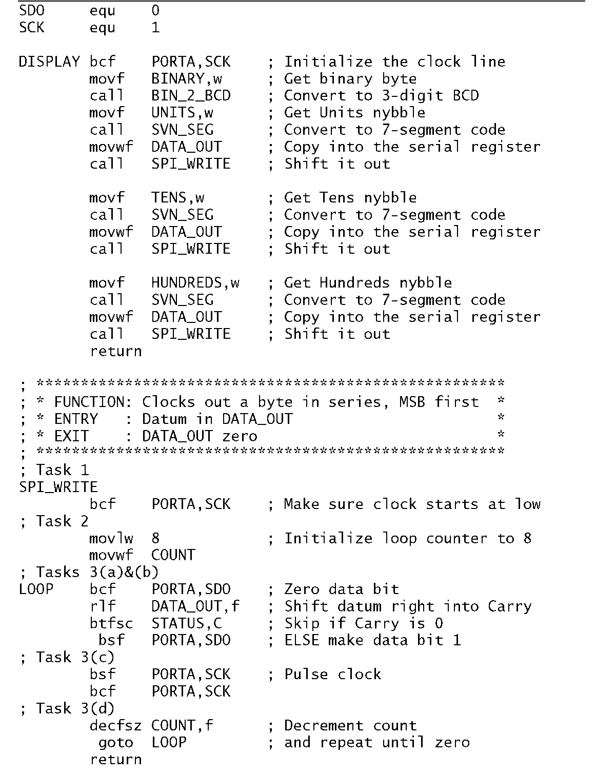
Program 12.1 shows two subroutines. The first called DISPLAY is closely akin to Program 11.7 in that it calls the subroutines BIN_2_BCD and then sends the 7-segment coded bytes out to the interface registers. In this instance the units byte is sent first as this will eventually be shifted to the far end of the chain; followed by the tens and finally the hundreds byte.
The actual serial transmission is handled by the subroutine SPI_WRITE, which implements our task list. The datum placed by the caller in file register DATA_OUT is shifted left and the state of the Carry bit used to make the Serial Data Out pin RA0 0 or 1. The Serial ClocK pin RA1 is then toggled once _![]() to shift the data into the shift register chain. This is repeated eight times to complete the transaction, which takes a maxi-mum of 87 cycles to complete, depending slightly on the data pattern. A complete update of the display will take around 120 ^s with a processor clock of 8 MHz and excluding the time spent in doing the data conversion.
to shift the data into the shift register chain. This is repeated eight times to complete the transaction, which takes a maxi-mum of 87 cycles to complete, depending slightly on the data pattern. A complete update of the display will take around 120 ^s with a processor clock of 8 MHz and excluding the time spent in doing the data conversion.
Program 12.1 Displaying the decimal equivalent of a binary byte using a serial data stream.
Where a long chain of shift registers is being serviced, speed may be improved a little if each register has its own data feed but all clocked with the same SCK pin or sharing the same lines but each with a separate Enable. This latter technique is the method used in Fig. 12.8.
One problem with our shift register technique is that for the period where shifting is in process the data appearing at the port outputs are not valid; for 23 clock pulses in our example. Of course in this situation the response of the eye to microsecond changes in illumination makes this observation spurious. However, this may not always be the case and in such instances the shift register may be buffered from the parallel outputs using an array of D flip flops or latches, which can be loaded after the shifting process has been completed to give a single update.
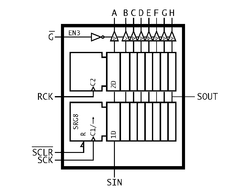
Fig. 12.3 Logic functional diagram of the 74HCT595 octal shift register with output register.
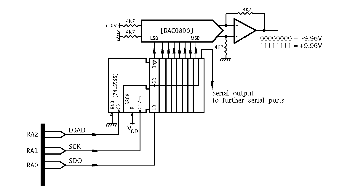
Rather than employing a separate buffer register, a more efficient solution typically uses the 74HCT595 of Fig. 12.3 with its integral 8-bit parallel-in parallel-out (PIPO) register between the shift register and the outside world. A rising edge _/ on the RCK (Register ClocK) pin transfers the serialized data to the parallel outputs. The last stage output of the shift register is made available to allow cascading to any length. All RCK pins can be pulsed together to allow the entire chain to simultaneously update.
One example where rippling of data may be undesirable, is were a digital datum is to be converted to its analog equivalent. In Fig. 12.4 the conversion is carried out using a National Semiconductor DAC0800. Essentially the analog voltage is a linear function of the 8-bit digital input varying from -9.96 V for an input of![]() through +9.96 V for
through +9.96 V for![]() - see Fig. 14.13.
- see Fig. 14.13.
Fig. 12.4 Serially interfacing to a DAC0800 digital to analog converter.
Using a 74HCT595 registered shift register, the digital input does not change until the new datum is in place and the PIC pulses the C2 Register Clock, giving clean changes in the data presented to the DAC and corresponding analog output.
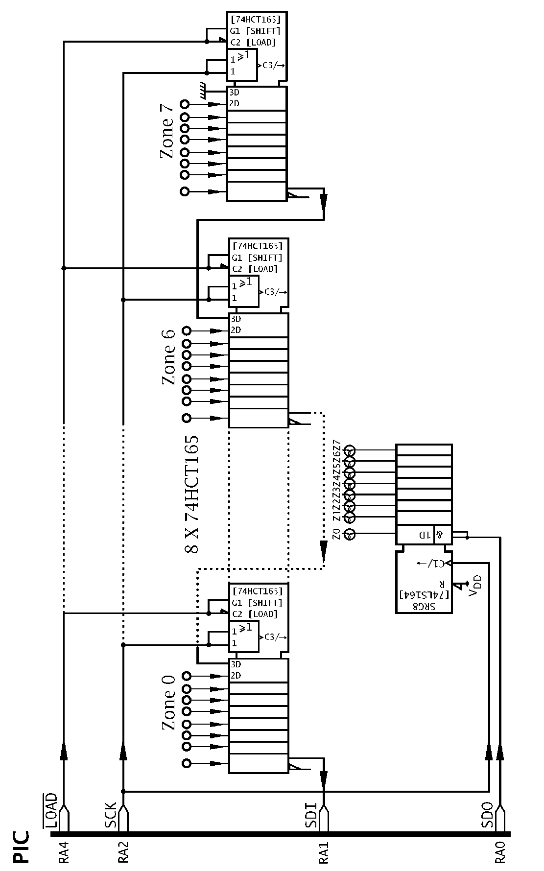
Data can be input serially in a similar manner using parallel-in serial-out (PISO) shift registers. The example shown in Fig. 12.5 is a serialized version of the intruder alarm of Fig. 11.10 using only three lines to connect to all eight sensor groups; a considerable economy compared to the original 16 channels.
Each sensor group is attached to a 74HCT165 8-bit PISO shift register, with the serial output of the further register feeding the serial input of the next nearest register. Once the data has been loaded in, it may be shifted into the SDI (Serial Data In) parallel input RA1 and assembled bit by bit. In the specific case of the multi-zone intruder alarm, after each eight shifts the assembled byte can be tested for non zero and the appropriate action taken – see SAQ 12.1.
Also shown in Fig. 12.5 is the single output port used to display the active zone. As both input SDI and output SDO serial channels share the same shift clock SCK, then shifting data in will also clock this serial output port. Conversely, sending data to the output port will shift data in from the Zone ports. In this example there is no problem as microsecond fluctuations in the Zone lamps are of no consequence, and the sequence of operations ends with the output port being accessed with the earmarked data. Where this interaction is undesirable, then either the appropriate datum should be continually presented to SDO at at the same time as it is read in at SDI or a latched register, such as the 74HCT595, used to staticize the display data. As an alternative, separate serial clock lines could be used.
Fig. 12.5 Serially interfacing to the multi-zone intruder alarm.
The core serial interface software is the input counterpart of subroutine SPI_WRITE in Program 12.1, which implements the following task list:
1. Bring SCK low.
2. COUNT = 8.
3. WHILE COUNT>0 DO:
(b) Copy input SDI to Carry.
(c) Shift left Carry into DATA_IN.
(d) Decrement COUNT.
