Besides setting CCP1IF and depending on the setting of the CCP1M[3:0] mode bits, one of four actions are possible on Timer 1 matching CCPR1:
Fig. 13.6 The CCP1 module set to Compare mode.
Pin RC2/CCP1 is forced high. 1001:
Pin RC2/CCP1 is forced low. 1010:
Pin RC2/CCP1 unchanged, but CCP1IF still set. 1011:
Timer 1 is cleared and with CCP2 only7 an analog module conversion is initialized by setting GO/DONE – see Fig. 14.8.
Where RC2/CPP1 or RC1/CCP2 are to be used as CCP outputs then the appropriate TRISC bit(s) should be cleared to set the pin direction to output. There is no way to directly reset or set the CCP latch other than zeroing the CCPCON register which resets the latch and disables the CCP module. In this case the state of the RC2/CCP1 pin will be that of PORTC[2] until the module is set to an appropriate mode, in which case the pin will reflect the state specified above when the match occurs.
As an example consider that we wish to set up Timer 1 as configured in the last example to generate an interrupt each 10 seconds. To do this we need set the timer to time-out after 16 s (prescale ratio 8:1) and then shorten the cycle. This is implemented by loading the CCPR1 register with the fraction y| – 1, which translates to 9FFFh. Whenever Timer 1 reaches this value it will automatically be reset on the next clock input (that would have normally incremented the timer to A000h) and an interrupt will occur if the CCP1IE mask bit (and global PEIE and GIE masks) are set. Initialization code for this is:
The PIC will then automatically be interrupted every ten seconds.
As CCP1 is not changed by Compare mode 1011 this pin can be used as a normal PortC input/output independently of the CCP1 module.
Where there are two CCP modules they can work in tandem using different modes, but the timebase will be common – see Example 13.3.
7This is the only functional difference between CCP1 and CCP2.
Modes 0100 – 0111 configure the appropriate CCP module to capture the state of Timer 1 when an ‘event’ occurs at the appropriate CCP pin. We can see from Fig. 13.7 that an event can be a falling or rising edge on the RC2/CCP1 pin or every 4th or 16th rising edge according to the CCP1M[3:0] mode bits. This Event prescaler is cleared when the mode bits are set to 0000.
Once a defined event has taken place the 16-bit state of Timer 1 is parallel loaded into the CCP register 1 and CCP1IF set. The processor can then subsequently read this frozen value – that is the time. If Timer 1 is reset after each capture then the sampled datum is the time since the last event. Alternatively, as Timer 1 continues to increment, its captured value can be subtracted from the previous reading to give the difference. As the mode may be altered on the fly, the time between rising and falling edge on CCP1 can be measured by toggling CCP1M[0] between captures. This may cause the CCP1IF flag to be set. To prevent false interrupts, CCP1IE should be cleared before the change-over and CCP1IF after the change-over. Alternatively, the CCP1 module can be used to capture the rising edge and CCP2 the falling edge – see Example 13.3. There is no room for the CCP2IF and the associated interrupt mask CCP2IE mask bit in PIR1/PIE1. Instead bit0 of PIR2/PIE2 are pressed into service and in many mid-range processors is the only occupant of these registers.
As our example, consider that we wish to measure the period of our ECG signal with the peak detector connected to pin CCP1. If we assume Timer 1 is clocked by its own 32.768 kHz watch crystal, our set up code is something like this:
Fig. 13.7 Capturing the time of an event.
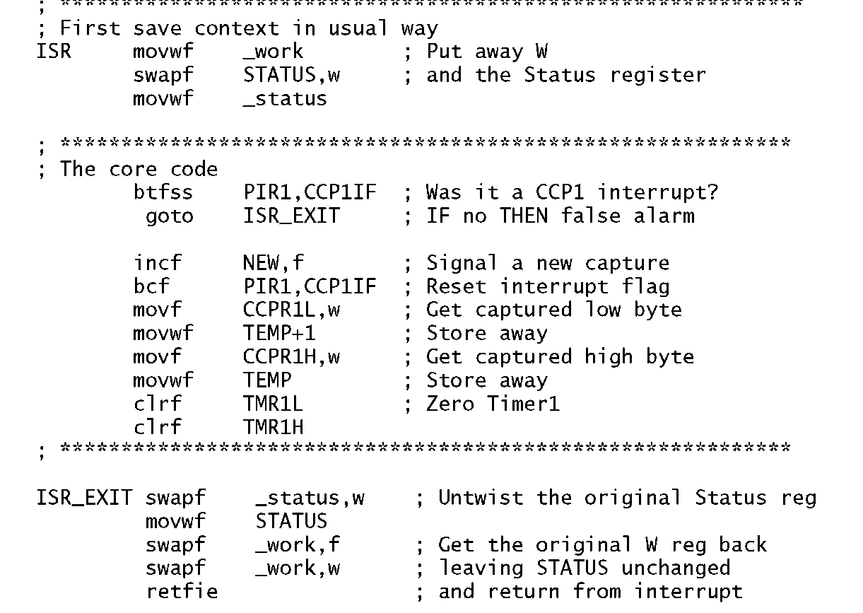
The ISR simply reads the contents of the CCP register and stores it away in two temporary locations, setting the file register NEW to indicate to background program that a new time datum exists. Timer 1 is then reset ready for the next event.
With a crystal of 32.768 kHz the time resolution of the captured datum is 30.5 /is with our 1:1 prescale setting. Timer 1 will overflow in 2 s, which is sufficient to record a heart rate of 30 beats per minute.
Program 13.4 Capturing the instant of time an ECG R-point occurs.
A more robust software system would also enable the Timer 1 overflow interrupt. if this occurs it indicates that the subsequent captured data will be invalid – although time-outs can be counted and thus extend the validity of the captured time. However, in our system it is more likely to be used to set off an alarm!
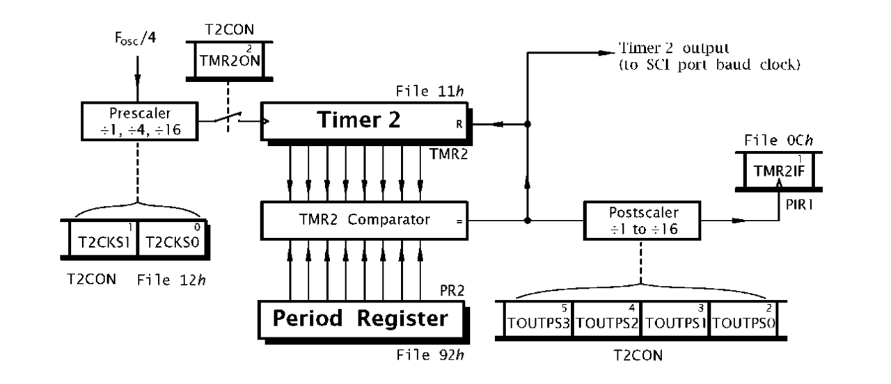
Timer 2 is an 8-bit counter which has both pre and postscalers. Unlike the two previous timers, output is not taken from the counter chain but from the Timer 2 Comparator. This compares the state of Timer 2 with that in the Period Register PR2. On equality an output pulse is generated which resets Timer 2 at the next clock pulse. This reset signal also sets the Timer2 Interrupt Flag TMR2IF in PIR1[1]. The number of equality events to set TMR2IF and optionally create an interrupt, is a function of the postscaler. Any integer number between 1 and 16 events can be set up using the TOUTPS[3:0] (Timer 2 OUTput Post Scaler) in the Timer 2 CONtrol register at T2CON[5:2]. T2CON at File 12h also controls the prescaler, giving four divide ratios for the internal clock, and can also be used to disable the timer. The reset state of T2CON is all zeros, disabling the timer and giving a pre/post scaler ratio of 1:1.
The advantage of this architecture is that time-out can be fine tuned by setting the Period Register to an appropriate value, independently of a CCP module. The period until TMR2IF is set is given as:
For our example, consider the need for an interrupt 100 times per second to scan a 7-segment display (see Program 11.8) and that the main crystal is 4 MHz. Choosing a prescale ratio of 4:1 gives a clocking period for Timer 2 of 4 is. If the Period Register is set to 249 then the Timer 2 comparator output period is 250 x 4 = 1ms. Thus setting the postscaler to 1:10 (1001) will give a 10ms (100Hz) interrupt rate.
Fig. 13.8 A simplified equivalent circuit for Timer 2.
By varying the postscaler from 1 to 16 (TOUTPS[3:0] = 0000 to 1111) respectively we can have an interrupt rate from 1 to 16 ms. For fine adjustments a unit change in PR2 alters the rate by 4 x postscaler x is. Set up code for this example is:
One of the more common applications of MCU-based systems is the control of power circuits, such as heating, lighting and electric motor speed control. One approach to this problem would be to use a digital to analog converter, such as that discussed in Fig. 12.16, driving a power amplifier. Linear control is expensive and inefficient due to the large current:voltage products that must be handled by the power amplifier. A rather more efficient and more cost effective approach rapidly switches the load on and off at a reasonably fast rate. A power switch, such as a thyristor, dissipates relatively little power, as when the switch is off no current flows and when the switch is on the voltage across the switch is low – ideally zero.
An example of such a waveform is shown in Fig. 13.9. The average amplitude is simply A x N%, where N is the duty cycle percentage of the repeat period. If we vary N from 0 to 100% then the average power will vary in a like fashion – all without the benefit of analog circuitry. This digital to analog conversion technique is known as pulse width modulation (PWM).
The thermal or mechanical inertia of most high-power loads is such that even with a relatively low repetition rate (typically no lower than 100 Hz) the ‘bumps’ will be smoothed. Low switching rates are more efficient, as each switching action dissipates energy. If PWM is used for more conventional digital to analog conversion, such as for audio, then a low-pass filter may be utilized to reduce the high-frequency harmonics. In such cases a sampling rate of at least ten times the maximum analog signal should be used to space out the harmonics (see Fig. 14.3) and reduce the necessary filtering burden.
Fig. 13.9 Pulse width modulation.

![tmp9295_thumb[2] tmp9295_thumb[2]](http://what-when-how.com/wp-content/uploads/2011/06/tmp9295_thumb2_thumb.png)

![tmp9297_thumb[2] tmp9297_thumb[2]](http://what-when-how.com/wp-content/uploads/2011/06/tmp9297_thumb2_thumb.png)


