RS-232 was originally designed for DTE-modem interconnection, although its use is now much more varied – see Fig. 12.21. Figure 12.20(d) shows a simple Frequency Shift Keying (FSK) full duplex system with the mark/space of one channel being represented by the tones 1070/1270 Hz and the other by 2025/2225 Hz; frequencies which fit well inside the normal telephone link bandwidth of 300 – 3400 Hz. Handshake lines DCD (Data Carrier Detect), CTS (Clear TO Send) and RTS (Ready To Send) are used to control the sequence of operations prior to and terminating the communication of data.
Many modem schemes currently use Phase Shift Keying (PSK) where typically at least eight different phases in 45° steps of a single tone are used to encode 3-binary bit code groups (tri-bits) in any one time slot. In this way the baud rate may be increased with the same signalling rate, albeit at the expense of noise immunity, as witnessed by the steady increase in PC-based home telephone internet data rates in recent years up to 56kbaud.
As an example, Fig. 12.21 shows the connection between a PIC and the serial port of a PC – or any device with an asynchronous RS-232 port. The Maxim MAX233 dual RS-232 transceiver translates from +12 V to 0 V (logic0) and -12V to +5V (logic 1). If handshake lines are not being used, as is usual in simple links, the PC can be ‘fooled’ into treating the interface as ready to accept data by linking as shown in the diagram. For instance, the serial port UART’s RTS is looped back to CTS. The MAX233 has two transmit and two receive buffers in all and thus can be used to buffer some additional handshake lines if required.
Fig. 12.21 Communicating with a PC via an RS-232 link and the outside world.
In Fig. 12.21 the same PIC is shown driving a half duplex RS-485 link using a Maxim MAX485 voltage converter. Each buffer has a separate Enable of the opposite logic polarity. The PIC can activate the appropriate buffer depending on the communication direction. Alternatively the MAX485 can be used to implement a full duplex channel using two separate links.
The RS-485 link need not use the asynchronous protocol. Any suitable synchronous protocol can be buffered to RS-485, but of course a separate clock channel will be needed.
Examples
Example 12.1
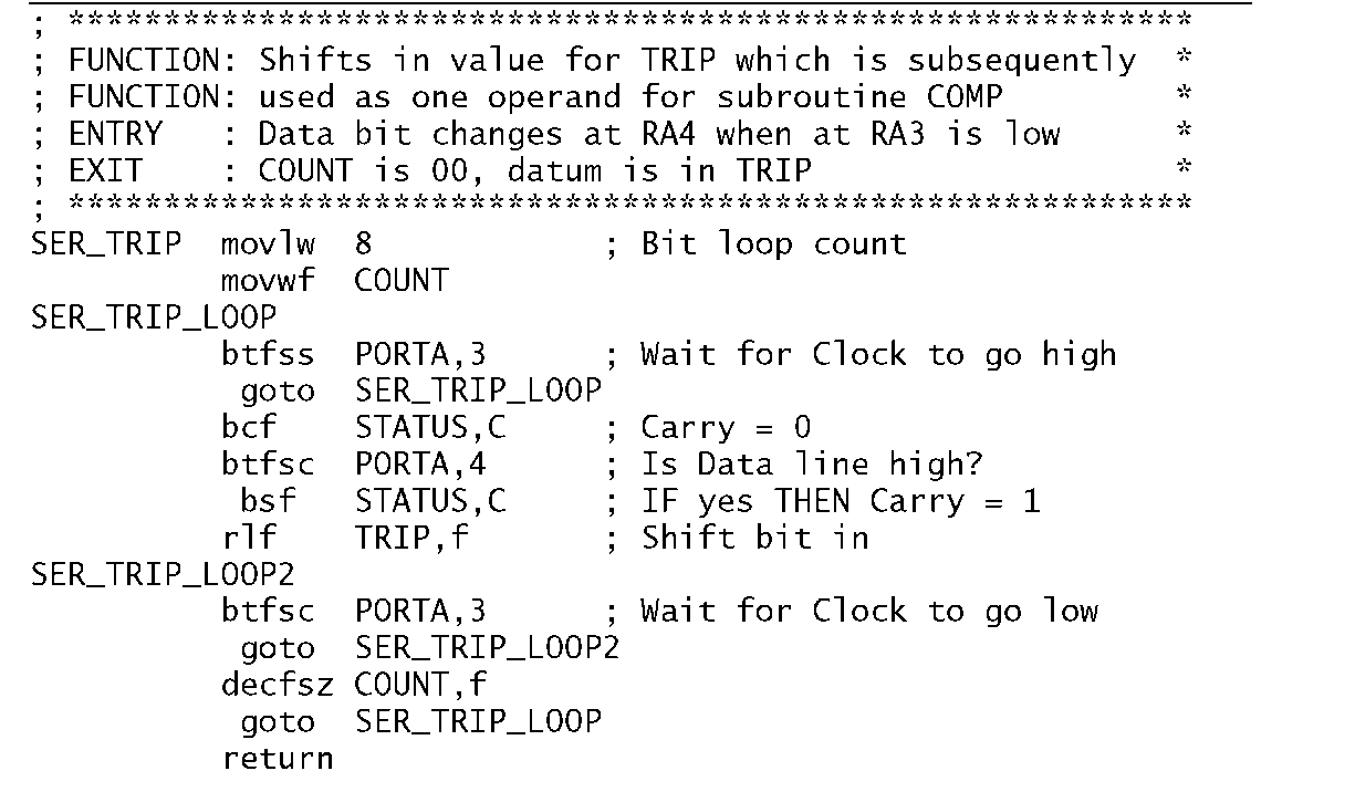
In Example 11.2 we designed a subroutine to compare a fixed number TRIP with the byte read in from Port B. In some cases it may be necessary to have the software adapt to changing circumstances, altering the trigger value by reading updates from outside. Rather than using up another eight port lines it is proposed that the update be fed in from an outside agency in series at pin RA4, with RA3 being used as the clock line. With the assumption that each data bit is set up when the Clock line is low write a subroutine to read in a new value into memory at TRIP.
Solution
One solution is shown in Program 12.13. The Clock line is monitored for high, during which time the Data is stable. By mirroring the state of the Data line into the Carry flag the datum is rotated bit by bit into memory.
After each shift the loop is not completed until the Clock line again goes low.
This is similar to subroutine SPI_READ in Program 12.2 except that the clock is generated from outside; that is the PIC is acting as a Slave. This causes problems in a real system where the PIC Slave must be able to tell the Master when it wants a new byte. This could be done by using another port line as a Clear To Send handshake which will interrupt the Master and initiate the conversion. Of course the Master could be another PIC and if so we have an economical way of connecting two PICs together. If PICs with integral serial ports are used then interrupts can be automatically generated and this is a frequently used way of implementing multi-processor networks.
Program 12.13 Updating Program 11.4′s trip value.
Example 12.2
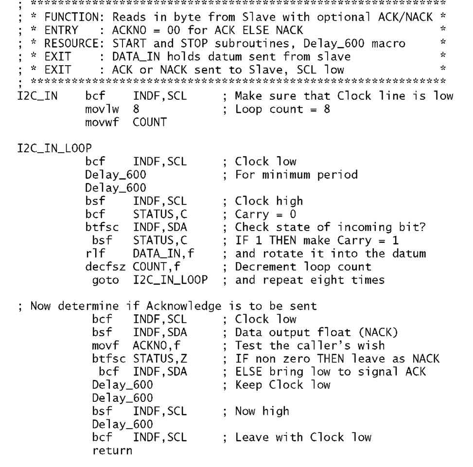
Design and code the I2C_IN counterpart of the I2C_OUT subroutine of Program 12.7. You may assume that the same variables are available and that the output datum is in DATA_IN on entry.
Solution
The I2C_IN subroutine of Program 12.14 shifts the datum in file register DATA_IN through the Carry flag eight times with pin SDA mirroring this bit state. At the same time the Clock line SCL is toggled in according to the I2C time and protocol specification as in our I2C_OUT subroutine of Program 12.7. In this protocol the Master signals back to the Slave to stop sending data by letting the SDA line float high in the Acknowledge slot in the ninth clock pulse – see Fig. 12.13. The normal low state in this slot is called ACK, whilst the deviant high Acknowledge state is called NACK (No ACKnowledge). To cope with both these situations our I2C_IN optionally generates either situation depending on the state of the variable ACKNO set by the caller. If file register ACKNO is zero on entry then a normal low ACK is sent in this slot. Any non-zero value in this variable causes a high NACK to be sent back to the Slave. The Slave then terminates its transmission and listens for the next Stop/Start condition.
Program 12.14 Reading in a byte using the I2C protocol.
Example 12.3
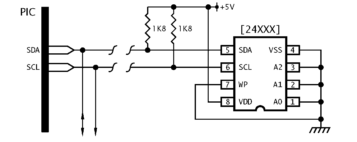
Many MCU-based products require storage of data in non-volatile memory for retrieval after the system has been powered down. A typical example is the total distance travelled by a car from new, which should be held independently of the state of the car battery. Such data is typically held in Electrically-Erasable Programmable Read-Only Memory (EEPROM) as described. Many EEPROM devices are available which interface to SPI and I2C, specifically the I2C 24LCXXX shown in Fig. 12.22. The 24LCXXX 8-pin serial EEPROMs vary from the 1 kbit 24LC01B to the 256kbit 24LC256, organized as bytes; i.e. 128byte to 32kbyte.
Fig. 12.22 The 24XXX series of I2C serial EEPROMs.
The 24XXX serial EEPROMs have the following features.
• 400 kHz I2C compatible (VDD = 5 V), 100kHz at VDD = 2.5 V.
• Write protection (ROM mode) using the WP pin.
• 2 ms typical Write cycle time.
• 1,000,000 minimum10 Write cycle endurance per byte cell.
• 3 mA Write, 1 mA Read and 100 ^s standby current.
• Internal generation of high programming voltage.
Using a 24LC01B serial EEPROM, show how you could increment a number in the bottom three locations which represents the total distance in either miles or kilometers depending on the market. You may assume that the PIC is interrupted on each mile/kilometer and that this software is part of the interrupt handler. You have the resources of the subroutines of Program 12.7 and 12.14.
Solution
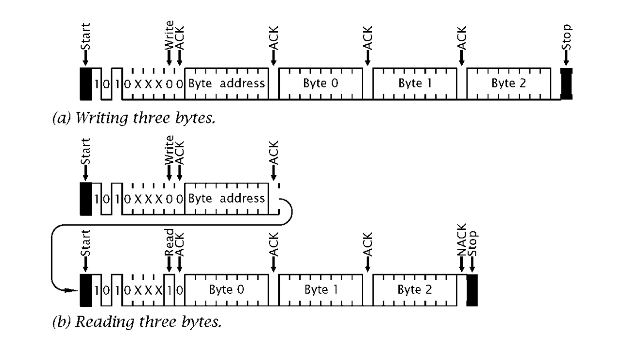
Before writing code to implement our specification we need to look more closely at the protocol used by the 24XXX serial EEPROMs in communicating with the Master PIC. This is encapsulated in the messages shown in Fig. 12.23.
In all cases the Master initiates a data transfer by sending a Start condition followed by a Command byte. The Control byte contains the I2C Slave address 1010; the chip select address A2 A1 A0 and the R/W bit in
the order![tmp9264_thumb222[2][2][2] tmp9264_thumb222[2][2][2]](http://what-when-how.com/wp-content/uploads/2011/06/tmp9264_thumb222222_thumb.png) Although the chip select address is shown as part of the Command byte and the three corresponding pins are shown in Fig. 12.22, newer versions of the smaller EEPROMS do not implement this feature. This is because if EEPROM capacity needs to be expanded then it more efficient to replace the device by a pin-identical larger version. For example replacing a 24LC01B by a 24LC08B gives an eightfold increase with no hardware alteration. Larger EEPROMS, such as the 24LC256 do implement chip select address as the method of expansion as additional devices will need to be hung on the bus in this situation. Eight 24LC256s will give a capacity of 256 kbyte of non volatile memory.
Although the chip select address is shown as part of the Command byte and the three corresponding pins are shown in Fig. 12.22, newer versions of the smaller EEPROMS do not implement this feature. This is because if EEPROM capacity needs to be expanded then it more efficient to replace the device by a pin-identical larger version. For example replacing a 24LC01B by a 24LC08B gives an eightfold increase with no hardware alteration. Larger EEPROMS, such as the 24LC256 do implement chip select address as the method of expansion as additional devices will need to be hung on the bus in this situation. Eight 24LC256s will give a capacity of 256 kbyte of non volatile memory.
This is normally followed by the address in the EEPROM that data is to be written into or read out of. In the specific case of the 24LC01B the data is arranged as 128 cells, each comprising a byte that can be individually written to or read from. This means that a 7-bit address will fit comfortably in the 8-bit address byte. This scheme will cope with devices up to the 24LC02B but beyond this addresses greater than 8 bit wide are needed. This is done by using the Chip select bits in the Command bit, giving an address width of 11 bits and a capacity of 2 kbytes (16 kbits). For EEPROMs larger than the 24LC16 two Address bytes are used following the Command byte.
The process of sending the byte address to the EEPROM is implemented as a Write action in Fig. 12.23. This is actioned by setting the R/W bit low in the command bit. Where a data byte is to be written into the addressed location this byte comes immediately after the Address byte and then followed by a Stop condition. If more than one data byte is transmitted before the Stop then this data is stored in a small on-board buffer and the actual programming will not occur until the Stop condition. The 24LC01B can store eight bytes at a time in a single page, with the lower three address bits being incremented on each data byte sent. If this address rolls over, earlier addressed data will be overwritten. The size of this page depends on the device; for example, the 24LC256 uses a 64-byte page. In Fig. 12.23(a) three bytes are shown being written into the 24LC01B. As these locations are to be targeted in the bottom three locations, 00-01-02h, then roll-over will not occur.
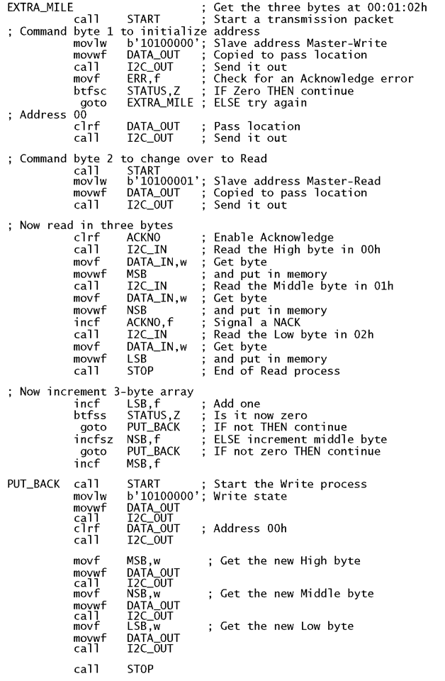
As soon as the Stop condition is received the 24LC01B will commence programming the targeted cells with the buffered data. This process takes typically 2-5 ms across the family. If the Master attempts to initiate a process during this time then the EEPROM will not Acknowledge following the Start-Control and byte and this can be used as a busy indicator. This polling is shown when the first Control byte is sent out in Program 12.15.
Program 12.15 Incrementing the non-volatile odometer count.
Fig. 12.23 EEPROM Read and Write waveforms.
The opposite process of reading bytes from the EEPROM is slightly more involved. As in the previous case a start address has to be written into the device. After this occurs a repeat Start condition is sent with the following Control byte having its R/W bit high to indicate Read. The Slave then transmits the byte at the specified location to the Master which Acknowledges receipt and the process continues indefinitely with the address incrementing until the Master does not send an Acknowledge. The Slave then releases the bus and the Master is free to issue a Stop condition. If the initial writing of the start address is omitted then one beyond the last used address is the additional location read from.
The software listed in Program 12.15 follows the process outlined in Fig. 12.23 exactly. Once the initial address 00h has been sent the Master goes into a listen mode and three sequential bytes are read from memory terminated by the Master by returning a NACK condition followed by Stop. With the triple-byte distance count in locations MSB:NSB:LSB the array is incremented in the usual way. Finally address 00h is again written out to the EEPROM followed by the three updated bytes and the process terminated by the Master transmitting Stop.

