At the end of the byte transfer, the Slave pulls SDA low to tell the Master that the data byte has been received. To allow this to happen the Master must release its control over SDA by allowing it to be pulled high via the bus resistor. Should the Slave not Acknowledge the transfer then the Master should abort the transfer and usually try again until timed out.
Several byte transfers will occur before the Master completes the transmission by bringing SDA high when the Clock is high. This Stop condition terminates the conversation. Another one can be initiated during the subsequent Idle state when the Master again sends out a Start bit. A Slave can distinguish the special Start and Stop situations, as this is the only time SDA changes when SCL is high.
The data transmission is framed between Start and Stop pairs and data flow can either be Master-Write as described or from Slave to Master in Master-Read mode. In the latter case it is the Master that acknowledges each byte. If it does not (No Acknowledge or NACK) then the Slave knows that the Master has finished and floats its SDA pin allowing the Master to output a Stop bit and then Idle both lines – see Fig. 12.23(b). It is possible for the Master to begin by writing data to the Slave and then request a change of direction. In this case a second Start bit is sent by the Master without stopping, followed by the appropriate control bits.
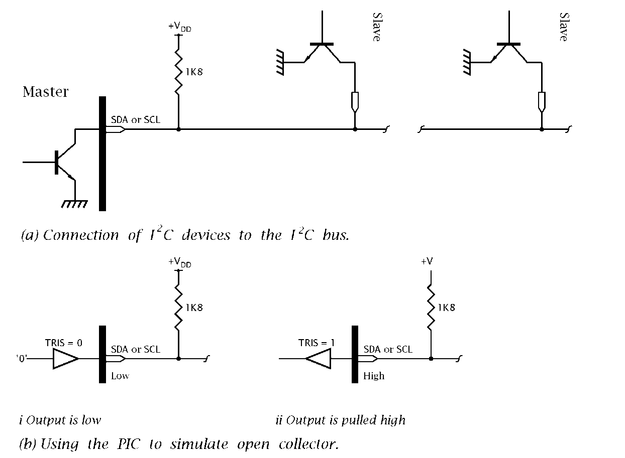
In using a PIC MCU to implement the I2C standard a problem arises as port outputs are not open-drain; that is the logic 1 output state is not open-circuit as required in Fig. 12.14(a). However, it is possible to get around this, simulating the high impedance state by switching the port line output to input. For example, if we wish to use RA2 as the SCL data line then to pulse SCL low and then high we have:
Fig. 12.14 Sharing the SCL and SDA bus lines.
where the high state is a consequence of the external pull-up resistor and the high input impedance, as shown in Fig. 12.14(b)//.
A complete transmission between Master and Slave comprises a packet of several byte/Acknowledge transfers sandwiched between a Start and Stop condition. To some extent the form of this packet depends on the requirements of the Slave device; however, all packets conform to the general sequence Slave address:Control/Command:Data shown in Fig. 12.15.
The essence of the I2C protocol is the requirement that each type of Slave device has an address. This address is allocated6 to the man-ufacturer of the I2C peripheral and is factory programmed. To allow more than one device of the same kind to share the same bus, most I2C-compatible devices allow two to four bits of this address to be set locally by the designer, usually by connecting Slave address pins to the appropriate logic levels. On receipt of a Start bit, all Slaves on the bus will examine the first seven bits for their personal address. If there is no match then the rest of the conversation is ignored until the next Start bit. Bit 8 is a direction bit, R/W is low if the Master is to be the transmitter and high if the Slave is to be the transmitter.
Fig. 12.15 A I2C packet transmission.
Not all 7-bit addresses are valid. All addresses matching![]() or
or![]() are reserved for special situations, leaving 224 valid addresses in total. Along with the introduction of a Fast mode, the I2C protocol was extended to permit a 10-bit address. This is signalled by the reserved address 11110XXb. In this case a second address byte is sent with the two XX bits in the first byte making up the total 10-bit Slave address.
are reserved for special situations, leaving 224 valid addresses in total. Along with the introduction of a Fast mode, the I2C protocol was extended to permit a 10-bit address. This is signalled by the reserved address 11110XXb. In this case a second address byte is sent with the two XX bits in the first byte making up the total 10-bit Slave address.
After the address byte(s), the next byte is usually treated by the addressed Slave as a Command/Control word, passing configuration information. For example a I2C memory may require the internal address where the data is to be written to – see Example 12.3. Bytes following this are usually pure data or a mixture of data and control bytes.
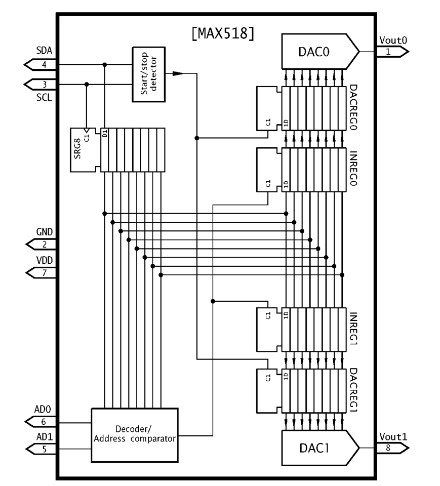
In order to illustrate these concepts we will use the Maxim MAX518 DAC, shown in Fig. 12.16, as our exemplar. This is the I2C counterpart to the SPI protocol MAX549, with a 2-layer register pipeline, two channels and a power-down feature.
The MAX518 has a 7-bit Slave address of the form![]() where AD1 and AD0 are the logic state of pins 5 and 6 respectively. If we assume that both pins are connected to GND then the Address byte sent out by the Master will be
where AD1 and AD0 are the logic state of pins 5 and 6 respectively. If we assume that both pins are connected to GND then the Address byte sent out by the Master will be with R/W being 0, as this device can only be written to.
The Command byte is of the form 000 RSTPDXXA0 with three active control bits: A0
Enables the input PIPO register for Channel 0 if 0 and Channel 1 if 1. PD
When 1 will power down both DAC channels, reducing the supply current to typically 4 ^ A. The contents of the internal registers remain unchanged and data may be shifted in and registers updated in this condition. The state information is only executed whenever a Stop condition is sent by the Master, when the last transmitted value of PD is acted upon.
Fig. 12.16 The MAXIM MAX518 I2C dual digital to analog converter.
RST
All internal registers are cleared irrespective of the following data byte which may be treated as a dummy byte. Analog outputs go to zero after the Stop condition.
In all cases the Stop condition updates the analog outputs according to the commands and data byte. If there have been several Command:Data byte pairs since the last Stop then the most recent command and data are reflected in the state and output of the device.
In order to interface to the MAX518 we will need to design subroutines to send out a Start condition, a Stop condition and a Master-Write byte. See Program 12.14 for a Master-Read subroutine. To design the device driver we need to look more closely at the time relationship between Clock and Data signals, which generally are more tightly defined than in the SPI protocol.
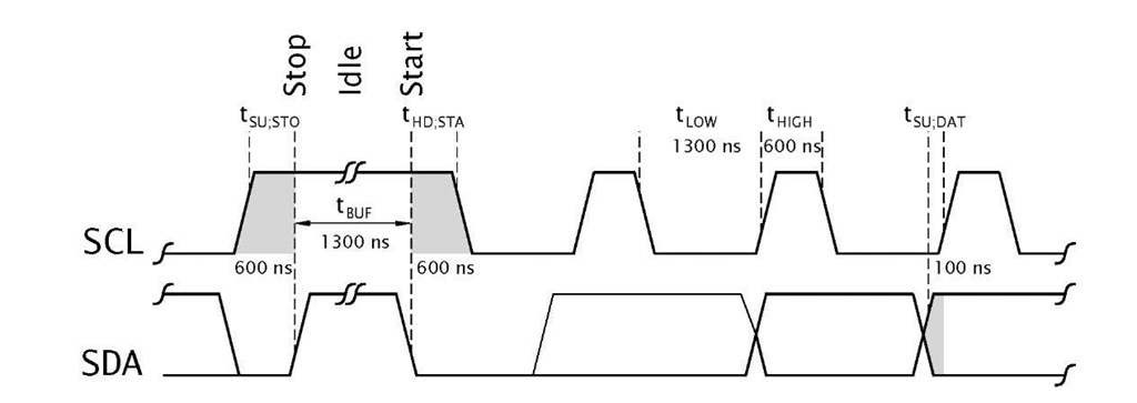
Fig. 12.17 Minimum timing relationships for the Fast I2C mode.
The MAX518 and most current I2C-compatible devices are designed to the Fast mode specification and the figures used in Fig. 12.17 relate to this 400 kHz clocking rate. Of particular note is the requirement that the clock SCL should be held high not less than 0.6 us (tHD;STA) after the active \_ of SDA to signal a Start condition. Similarly, a Stop condition requires that the clock be set up high at least 0.6 us (tSU;STO) before the active _/ of SDA. A minimum of 1.3 us is required with the bus free (tBUF) in the Idle state between a Stop and a following Start condition. These requirements allow time for the Slave devices to detect these synchronizing events without ambiguity.
During a data byte transmission the clock should be low no less than 1.3 us (tLOW) and high no less than 0.6 us within the 2.5 us overall duration limitation imposed by the 400 kHz. Data changes only when the clock is low, and any change should be complete no less than 100 ns (tSU;DAT) before the clock goes high.
Not shown in the diagram is the maximum rise and fall times which should not exceed 300 ns with a maximum bus capacitance of 400 pF. To keep within this transition restriction the pull-up resistors of Fig. 12.14 should not be more than 1.8 kQ with this value of capacitance. With short bus runs and few Slave devices this value of resistance can be increased by up to a factor of ten to reduce energy dissipation when an output pin is low.
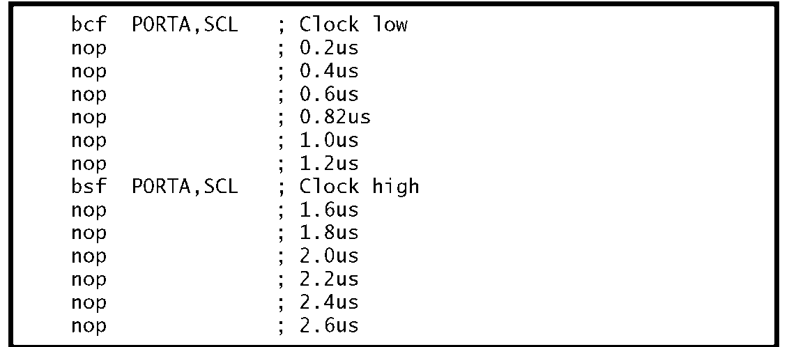
In implementing the I2C timings, a PIC with a crystal above 3.2 MHz, with an execution time of less than 1.25 ^s, may need to insert short delays between actions. For example, a 20 MHz crystal driven PIC implementing the instruction pair:
Would give high and low durations of only 0.2 ^s. Short delays are conveniently implemented using nop (No OPeration) instructions; each taking one instruction cycle (Fosc/4). For example, to give a nominally 400 kHz clock at 20MHz we have:
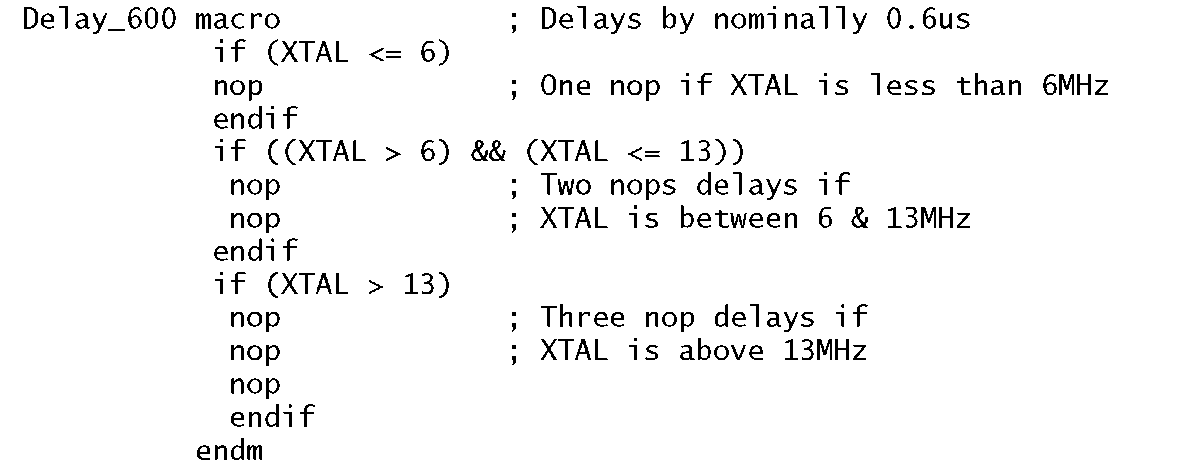
Of course slower clock speeds require less nops but rather than tailor our subroutines for one particular crystal we will use the assembler macro called De1ay_600, coded in Program 12.6, that will expand to the appropriate number of nops to give a nominal 600 ns (0.6 ^s) delay, depending on the value of the constant XTAL defined by the programmer at the head of the source file.
For example to alter the coding of Program 12.7 to suit a 12 MHz crystal system then the one line #define XTAL 20 should be altered to #define XTAL 12 and the program reassembled.
The coding of Program 12.6 makes use of the conditional assembly directive if – endif. This is similar to the C language statement if(true){do this;} in that all instructions down to the following endif are implemented if the argument of the if directive is true. For example, if((XTAL>6)&&(XTAL<=13)) states that if the constant XTAL is greater than 6 AND less than or equal to 13 then insert two nop instructions. At 13 MHz this will be approximately 600 ns. In practice, extra delays will be introduced by instructions toggling the bus lines and executing housekeeping tasks. Thus some fine tuning can be undertaken if maximum speed is a criterion.
Program 12.6 A crystal frequency-independent short delay macro.
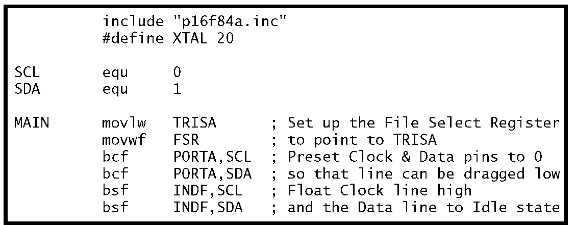
Based on the macro of Program 12.6 and the following initialization code:
Which assumes that we are using Port Abits 0 and 1 of a 20 MHz PIC16F84A to implement our SCL and SDA lines, we can code the three subroutines outlined in Program 12.7 to allow us to communicate with the I2C MAX518.
