Summary and Future Directions
Overall, in this section, we have shown that semiconductor NW materials can be doped p- and n-type in a precisely controlled way, and these electronically well-defined NW materials thus enable the assembly of a broad range of nanoscale electronic and optoelectronics devices, including FET, crossed NW p-n diodes, intra-NW p-n diode, bipolar transistors, cNW-FETs. Together, these devices represent a set of critical elements for the bottom-up assembly of more complex electronic circuits. To exploit best, this tool box of elements for building highly integrated electronic circuits will require several issues to be addressed, including: 1) production of device elements in high yield, 2) development of rational methods for assembly of these elements into integrated device arrays, and 3) development of system architectures that best utilize these device element function(s) and assembly capabilities. These important issues are further addressed in sections below.
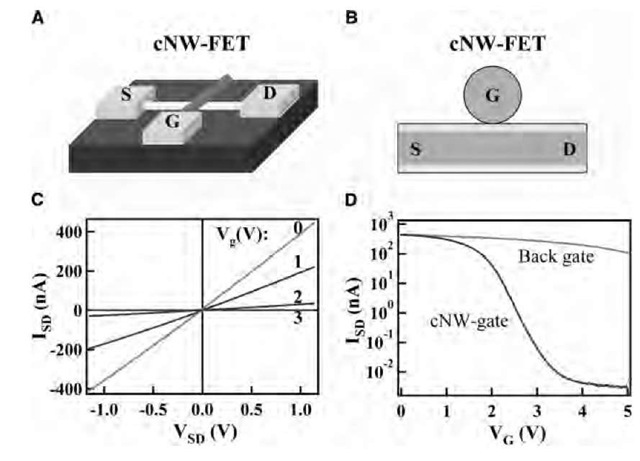
Fig. 10 Crossed NW-FET (cNW-FET). (A) Schematics illustrating the cNW-FET concept. A nano-FET with both nanoscale conducting channel and nanoscale gate is obtained with one NW used as the gate for the other NW in a crossed configuration. (B) Schematic showing the critical device dimensions of the cNW-FET. Three intrinsic nanometer scale metrics are naturally defined by the structure (see text). (C) Gate-dependent I-Vsd characteristics of a crossed NW-FET. The NW gate voltage for each I-V curve is indicated (0, 1, 2, and 3 V). (D) The curves showing I vs. Vg for n-NW and global back (light gray) gates for Vsd of 1 V.
The availability of electronically well-defined NW building blocks, which have enabled to demonstrate a series of nanoscale electronic devices, opens many exciting opportunities in nanoscale science and technology. For example, the nanoscale electronic devices may enable us to construct functional electronic circuits with integration density far beyond current technologies. The wide range of electronic applications described above are based primarily upon diffusive motion of electrons as in conventional devices—their uniqueness arises from the small size scale and our ability to obtain unique function from combinations of materials that would be incompatible with conventional fabrication processes. In addition, other effects, such as the quantum mechanical or wave-like nature of carriers, will need to be accounted for for sufficiently small structures,[15,42] and at the same time could open up entirely new possibilities for electronic manipulation and devices.[43]
The intrinsically nanometer scale devices assembled from NWs or NTs represent ideal systems to probe quantum phenomena and exploit devices exhibiting such phenomena for fundamentally new applications such as quantum computation.[44,45] The availability of a wide range of NW materials opens up considerable opportunity for exploring these exciting directions since fundamental properties, such as the Fermi wavelength and number of conductance channels, can be systematically varied through choice of NW material (e.g., InAs vs. Si) and diameter, respectively.
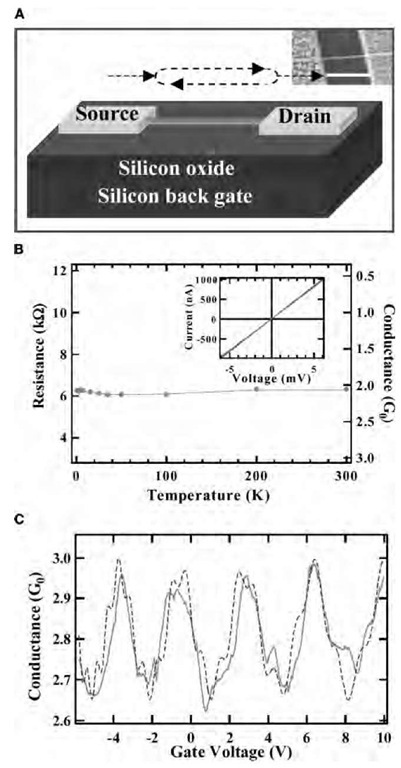
As an example of the potential of NWs to enable behavior not readily accessible with conventional planar devices, we consider recent studies of InAs NWs (Fig. 11A). Significantly, temperature dependent three-terminal transport studies show that the conductance of individual InAs NWs remain essentially unchanged over the temperature range from 300 K down to 1.6 K (Fig. 11B). The temperature independent transport suggests strongly that electrons are not inelastically scattered by either impurities or phonons within the NWs, that is, that the electron transport is ballistic. This important conclusion is supported by several other pieces of data, including 1) most of the InAs NWs exhibit conductance values ranging from one quantum conductance (G0 = 2e2/h) to 8G0 and 2) the conductance shows little or no dependence on NW length. We have also obtained similar results for clean Si NWs, and thus believe that the ballistic transport phenomena can be considered as a general property to exploit in NW-based nanoelectronics.
Fig. 11 Low temperature studies of InAs NWs. (A) Schematic showing an InAs NW device. Electron waves inside the NWs are partially reflected at the two metallic contacts, and the forward and backward reflected waves quantum mechanically interfere with each other. (B) Conductance vs. temperature of an InAs NW device. (C) Conductance vs. gate voltage (Vsd = 0.5 mV) at 1.6 K. The dashed line corresponds to a theoretical fit based on multichannel Landauer formalism discussed in the text.
Transport studies also suggest that InAs and Si NWs can exhibit coherent phenomena. Specifically, low-temperature gate voltage-dependent conductance measurements exhibit reproducible, quasi-periodic conductance oscillations (Fig. 11C). These oscillations can be interpreted as quantum interference between electron waves reflected by two metallic contacts, much like optical waves interfere within a Fabry-Perot cavity. In our NW electron cavities, the gate-voltage modulates the Fermi level, and hence changes the Fermi wavelength and the interference of the electron waves inside the NW. The observed electron-wave interference has been quantitatively analyzed using a multichannel Landauer formalism,[42,46] where the overall conductance is determined from two 6 x 6 scattering matrices representing the NW-metal contacts and one 6 x 6 transmission matrix inside the NWs.[45] Significantly, the calculated conductance behavior accounts for both major and minor oscillatory features in the data, and show that these different features arise from the different sub-band modes of relevance to the InAs NW cavity.
The unique transport properties of these InAs and similar NWs could lead to a number of exciting opportunities for devices and systems integration. For example, ballistic transport will be important to advance interconnects and highly integrated nano-systems since it eliminates power dissipation within the NW. Ballistic and coherent transport should also enable spin-dependent transport and spin-based devices.[47] Moreover, the ability of NWs to exhibit coherence over large distances—that is, transmit quantum mechanical information—should also be important in the emerging field of quantum computing.[44] In a quantum computer, the usual digital "bits” are replaced by quantum bits (qubits), and these qubits can be manipulated in very different ways by forming superpositions or entangled states, and thereby used to solve computing tasks inaccessible to digital systems. We believe that the availability of high quality NW materials opens up a new pathway for assembling quantum devices and potentially exploiting the potential of quantum computing.
NANOSCALE OPTOELECTRONICS AND PHOTONICS
In addition to nanoscale electronics, the broad range of optically active III-V and II-VI group compound semiconductor NW materials are attractive as building blocks for miniaturized photonic and optoelectronic devices. In this section, we review exciting progress in this area. First, we discuss results from fundamental photoluminescence (PL) studies of individual NWs. Second, we review assembly and properties of a wide range of photonic devices, including nanoscale LEDs, NW optical cavities, single NW lasers, and photodetectors.
Photoluminescence Studies of Individual Nanowires
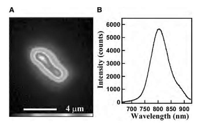
Photoluminescence studies on individual NWs reveal that they exhibit strong PL and can be readily imaged with a liquid nitrogen cooled CCD camera. For example, PL image of an InP NW clearly shows an elongate emission along the wire axis (Fig. 12A). The PL spectrum shows a peak maximum at ^805 nm in contrast to bulk value of ^925 nm (Fig. 12B). This large blueshift suggests the radial quantum confinement of excitons in the NW, which have been addressed in detail by size-dependence PL studies.[48]
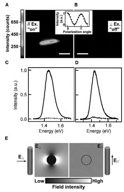
In addition to strong quantum confinement caused by the large confining potential for both electrons and holes, another unique feature of free-standing NW structures is the large variation in the dielectric constant between the NW and surrounding (air) medium, which could lead to strikingly new phenomena. For example, PL studies of individual InP NWs show that the PL intensity essentially turns from "on” to "off" as the excitation polarization is rotated from parallel to perpendicular (Fig. 13A,B).[49] Integration of the emission intensity as a function of excitation angle shows that the PL intensity exhibits a periodic dependence (cos2 6) on the angle. Photoluminescence spectra recorded from NWs of different diameters ranging from 10 to 50 nm show similar large anisotropy in either excitation (Fig. 13C) or emission polarization (Fig. 13D). In both cases, the ratio of parallel to perpendicular emission is greater than an order of magnitude, with a polarization ratio p = (I\\ — I?)/(I\\ + I?) of 0.91 ± 0.07. This large polarization ratio is significantly larger than previously reported (buried) quantum wire samples, where the polarization aniso-tropy has been attributed to the mixing of valence bands due to quantum confinement. This quantum mechanical effect yields a much smaller polarization ratio of p < 0.60[50-52] and cannot be used to explain the large polarization ratio in the free-standing NWs. Rather, the large and unprecedented polarization anisotropy in the free-standing NWs can be accounted for quantitatively by considering the dielectric contrast between a NW and its air or vacuum surroundings; that is, the perpendicular electric field amplitude is attenuated according to Ei = [2e0/(e + e0)Ee], where Ei is the electric field inside the cylinder, Ee is the excitation field, and e(e0) is the dielectric constant of the cylinder (vacuum) (Fig. 13E).[53] This model yields a theoretical polarization ratio, p = 0.96, in good agreement with the experimental results for InP NWs.
Fig. 12 Photoluminescence studies of individual NWs. (A) Room-temperature PL image and (B) spectrum from single InP NW.
Fig. 13 Polarized PL excitation and emission from individual NWs. (A) Photoluminescence image of a single 20 nm InP NW with the exciting laser polarized along the wire axis. Scale bar, 3 mm. (B) Photoluminescence image of the same NW as in (A) under perpendicular excitation. Inset: Variation of overall PL intensity as a function of excitation polarization angle with respect to the NW axis. (C) Excitation spectra of a 15 nm diameter InP NW. These spectra were recorded with the polarization of the exciting laser aligned parallel (solid line) and perpendicular (dashed line) to the wire axis. (D) Emission spectra of the same wire as in (C). These spectra were taken with the excitation parallel to the wire, while a polarizer was placed in the detection optics. (E) Dielectric contrast model of polarization anisotropy.
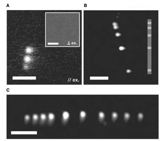
The strong polarized PL emission from individual NWs allows us to explore them for many exciting application in nanophotonics. For example, the previously described GaAs/GaP NW superlattice structures represent an attractive system for applications such as nanobarcodes because GaAs is a direct band gap semiconductor, while GaP has an indirect gap.[54] Indeed, PL imaging of individual NWs from the equally spaced (GaP/GaAs)3 superlattice sample shows that these NWs exhibit an emission pattern of three spots separated by dark regions (Fig. 14A). This pattern is consistent with emission originating from the three GaAs regions, separated by dark GaP regions that act as optical ”spacers.” Control experiments on individual samples of pure GaAs and GaP NWs confirm that strong luminescence is obtained from GaAs but not GaP, as expected. The GaAs regions also exhibit a strong polarization dependence, emitting when the excitation is polarized parallel (||) to the NW axis and appearing dark when the polarization is perpendicular (?) to the NW axis (Fig. 14A, inset).
Such superlattice systems can be further extended to more complicated structures. First, the PL image of an 11-layer superlattice in which the length of the GaP regions was doubled each layer while maintaining a constant GaAs period (Fig. 14B) shows clearly that the separation between emitting GaAs regions is doubling along the length of the NW. Second, the PL image of 21-layer GaP/GaAs superlattices (Fig. 14C) consisting of a short 4-period (GaP/GaAs) repeat, followed by three longer GaP spacer repeats, and ending in a relatively short 4-period (GaAs/GaP) repeat shows consistent PL patterns. We consider that, in their present form, these NW superlattice structures could be exploited as optical nanobarcodes, which could be useful as labels for imaging. Moreover, the wide range of group III-V and II-VI NWs that have been demonstrated previously suggests that it should be possible to encode additional information through variations in the color of the emitting region using multicomponent superlattices. Using materials with a large dielectric contrast might also enable the creation of 1D waveguides with built-in photonic band gaps, or of cavities for NW lasers.
Crossed Nanowire Light Emitting Diodes
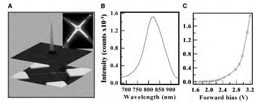
The observation of strong PL from individual NWs has stimulated further interest in exploiting such NWs for optoelectronics. We have previously described a wide range of electronic device assembled from NWs including p-n diodes. In direct band gap semiconductors like InP, the p-n diode also forms the basis for the critical optoelectronics devices, including LED and laser diode. To assess whether our nanoscale devices might behavior similarly, we have studied the electroluminescence (EL) from crossed NW p-n junctions. Significantly, EL can be readily observed from these nanoscale junctions in forward bias.[33] A three-dimensional (3D) plot of the EL intensity taken from a typical NW p-n diode at forward bias (Fig. 15A) shows the emitted light comes from a point-like source, and moreover, comparison of EL and PL images (Fig. 15A, inset) recorded on the same sample shows that the position of the EL maximum corresponds to the crossing point in the PL image. These data thus demonstrate that the emitted light indeed comes from the crossed NW p-n junction.
Fig. 14 Nanowire nanobarcodes. (A) Photoluminescence image (|| excitation) of a NW with a (GaAs/GaP)3 superlattice structure. The three bright and dark regions correspond to the three GaAs (direct band gap) and GaP (indirect band gap) regions, respectively. Inset: No PL is observed above background for perpendicular excitation. Scale bar, 5 mm. (B) Photoluminescence image of a 40 nm diameter GaP(5)/ GaAs(5)/GaP(5)/GaAs(5)/GaP(10)/GaAs (5)/GaP(20)/GaAs(5)/GaP(40)/GaAs(5)/ GaP(5) superlattice; the numbers in parentheses correspond to the growth times in seconds for each layer. Inset: Diagram showing the relative lengths of GaAs (blue) and GaP (red) layers. Scale bar, 5 mm. (C) Photoluminescence image of a 21-layer superlattice (GaP/GaAs) 10GaP, showing a group of four equally spaced spots on the left, two in the middle with larger gaps, and another set of four with equal spacing on the end. The superlattice is 25 mm in length.
Characterization of the EL intensity as a function of forward bias of the junction shows that significant light can be detected with our system at a voltage as low as 1.7 V (Fig. 15B). Further increases in forward bias beyond this ”turn-on” voltage produce rapid increase in the EL intensity. In addition, EL spectra recorded from the cNW-LEDs exhibit blueshifts relative to the bulk band gap of InP (925 nm) (Fig. 15C). The blue-shifts are due in part to quantum confinement[55] of excitons, although other factors may also contribute. Furthermore, PL studies have demonstrated that the PL peak can be systematically blueshifted as the NW diameter is decreased,[48] and thus these results provide a means for controlling the color of the LEDs in a well-defined way. Indeed, EL results recorded from p-n junctions assembled from smaller (and larger) diameter NWs show larger (smaller) blueshifts. In addition, the emission color from nano-LEDs can be further varied by using chemically distinct semiconductor NWs with different band gaps. Considering the wide range of group IV, III-V, and II-VI semiconductor NW materials available,[30] it is possible to assemble a variety of NW-based nano-LEDs for different spectral regimes.[41] The ability to tune color with size as well as composition in these nano-LEDs might be especially useful in future nanophotonic applications. Moreover, the nanoscale light emitting device can be flexibly assembled on virtually any substrate and seamlessly integrated together, and allows us to achieve unique optoelectronic function on many technological important substrates, such as silicon substrate, and can open entirely new opportunities in intra-/interchip optical communication, integrated chemical/biological sensing and medical diagnostics on the chip level.
Fig. 15 Crossed NW LED. (A) (Top) Three-dimensional (3D) plot of light intensity of the EL from a crossed NW LED. Light is only observed around the crossing region. (Bottom) Three-dimensional atomic force microscope image of a crossed NW LED. Inset: PL image of the crossed NW junction. (B) Spectrum of the emission shows a peak at ca. 820 nm. (C) Plot of integrated intensity vs. forward bias voltage.
Single Nanowire Nanolasers
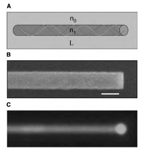
Semiconductor lasers are finding increasing use in technologies ranging from telecommunications and information storage to medical diagnostics and therapeutics. Free-standing semiconductor NWs are attractive building blocks for creating optically and electrically driven lasers since their defect-free structures exhibit the superior optical and electrical transport properties,[32-35] and because a single NW can function as a stand-alone optical cavity and gain medium.[56-58] In general, a NW will function as a single mode optical waveguide[59] (Fig. 16A) when 1 – (pD/1) (W12 — n02)0 5 < 2.4, where D is the NW diameter, l is the wavelength, and n1 and n0 are the refractive indices of the NW and surrounding medium, respectively. Taking CdS NWs (n1 = 2.5; l = 510 nm, 300 K) as an example, the minimum diameter needed to support a single mode is of the order of 70 nm. If the ends of the NW are cleaved, they can function as two reflecting mirrors that define a Fabry-Perot optical cavity with modes m(l/2n1) = L, where m is an integer and L is the length of the cavity. Significantly, CdS NWs typically adopt a [0 0 1] direction along the axis and can be easily cleaved using solution phase sonication. Transmission and scanning electron microscopy studies show that the cleaved NW end exhibit flat ends (Fig. 16B) indicative of cleavage perpendicular to the [0 0 1] NW axis. A luminescence image of a cleaved CdS NW obtained with a fluorescence microscope under uniform illumination from a mercury lamp shows uniform emission along the entire NW body except the end where greatly enhanced emission is observed (Fig. 16C). The uniform emission from the NW body suggests high quality of the NW materials, and the enhanced emission near the NW end suggests that the NW can function as waveguide.
Fig. 16 Nanowire optical waveguides and cavities. (A) Schematic showing a NW as an optical waveguide; with cleaved ends, it defines a Fabry-Perot cavity. (B) SEM image of a cleaved CdS NW end. Scale bar, 100 nm. (C) Room-temperature PL image of a CdS NW uniformly excited with a mercury lamp.
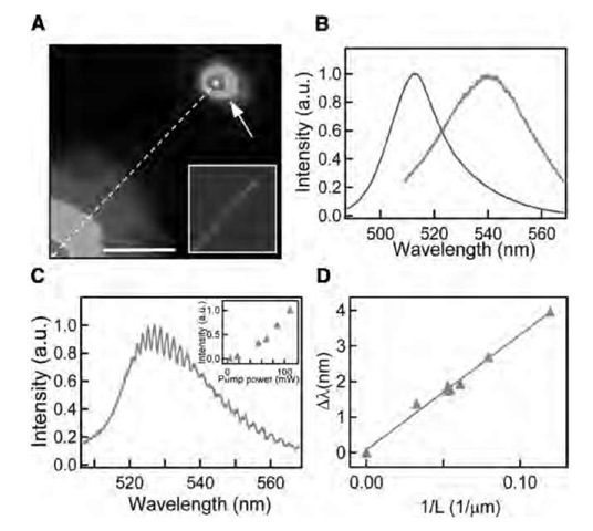
The optical cavity properties of the CdS NWs, which are central to our use of these nanostructures for lasers, were further characterized by PL measurements at the single NW level using a far-field epi-fluorescence microscope. A typical room-temperature luminescence image (Fig. 17A) of a CdS NW excited with a tightly focused laser ca. 15 mm from the NW end shows strong emission at the excitation locus and also prominent emission near the NW end. Studies of a number of NWs show pronounced emission from the NW end in addition to the excitation region and thus confirms waveguide characteristics of the NWs.
To further probe the NW cavity properties, spectro-scopy measurements have been made at different regions as a function of excitation power under uniform illumination. At low power, PL spectra recorded from the body exhibit a broad peak with a maximum at 512 nm and full width at half maximum (FWHM) of 24 nm (Fig. 17B). The peak maximum is consistent with room-temperature band edge emission from CdS, and contrasts the deep level emission around 600 nm that usually dominates epitaxial CdS thin films.[60] Spectra recorded from the NW end at low excitation power showed a relatively broad peak that was redshifted ca. 30 nm relative to spectra from the body. The observed spectral redshift is consistent with reabsorption of band edge emission within the CdS NW cavity.
Fig. 17 Nanowire Fabry-Perot optical cavity. (A) Room-temperature PL image of a CdS NW excited ca. 15 mm away from the NW end. The white arrow and dashed line highlight the NW end and axis, respectively. Scale bar, 5 mm. Inset shows an optical image of the NW obtained with white light illumination. (B) Photoluminescence spectra obtained from the body of the NW (left) and the end of the NW (right) at low pump power. (C) Spectrum from the NW end at higher pump power (80 mW) exhibiting periodic intensity modulation, which corresponds to the Fabry-Perot modes of the NW. Inset shows end emission intensity as a function of pump power. (D) Mode spacing vs. inverse NW length. The triangles are experimental point except the origin (0,0) point that corresponding the extrapolation to infinite length; the line is linear fit to these data.
Photoluminescence measurements made at higher excitation powers reveal other important features about the CdS NW cavities (Fig. 17C). First, the NW end emission blueshifts towards the band edge as the reabsorption is partially saturated with increasing excitation power. Second, the end emission intensity increases superlinearly with excitation power, while emission from the NW body exhibits a slight ca. linear increase. Third, periodic variations in the intensity, which are suggestive of the longitudinal modes of a Fabry-Perot cavity, are observed for excitation powers greater than the changeover from linear to superlinear behavior. For a cavity of length L, the mode spacing, AA, is given by A2/2L[n1-A(dn1/dA)]—1, where dn1/dA is the dispersion relation for the refractive index. This expression provides a good description of the observed spacing when the measured NW length is equated with L, and moreover, analysis of similar data from NWs of varying length demonstrates that the mode spacing is inversely proportional to the wire length (Fig. 17D) as expected. Together these results show that the CdS NWs form a Fabry-Perot cavity with a cavity quality factor of the order of 600 as estimated from the mode line width.
The observation of sharp modes in the uniform CdS NW gain medium above the superlinear threshold is indicative of amplified spontaneous emission. Significantly, excitation at higher powers, which was possible in low-temperature experiments, leads to preferential gain in a single mode and the onset of lasing (Fig. 18A). At low temperatures, the broad emission peak observed at the NW end rapidly evolved to a sharp single mode with the 0.7 nm line width limited by the resolution of our low-temperature instrument (Fig. 18B). The observed line width exhibits a sudden drop in line width to our instrument resolution at an excitation power coincident with the threshold to superlinear dependence for emission (Fig. 18C). In contrast, emission from the NW body is broad and linearly dependent on excitation further demonstrating that the laser emission is due to the cavity along the NW axis. From this superlinear behavior, we estimate the threshold average pump power to be 40 kW cm—2, although the threshold varies from NW to NW with the lowest value to date of —10kWcm—2.
These optical experiments demonstrate that individual NWs can function as Fabry-Perot cavities and support lasing, although without electrical pumping NW lasers would be of limited technological importance. In general, electrically driven lasing requires efficient electron (n-type) and hole (p-type) injection into the cavity region. In the case of planar CdS structures, this has been difficult due to problems in producing high-mobility p-type CdS or combining n-CdS with other high-mobility p-type materials. A clear advantage of NW-based structures is the ability to combine different high quality materials almost at will to achieve desired device function.
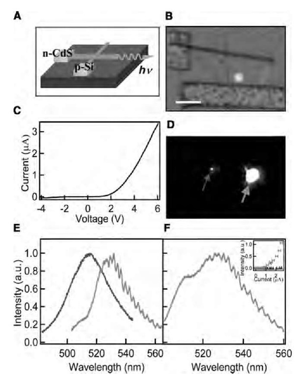
Our initial studies of electrical injection into CdS NW cavities were carried out using an n-type CdS and p-type silicon (p-Si) crossed NW structures (Figs. 19A,B). Transport studies of individual CdS NWs show that they are n-type with doping concentrations of the order of 1018-1019/cm3 and electron mobilities of ca. 100cm2/Vsec; the p-type silicon NWs had a doping concentration of ca. 1018-1019/cm3 and exhibited mobilities of ca. 50-300 cm2/V sec. Current-voltage (I-V) measurements made on a typical n-CdS/p-Si crossed NW structure (Fig. 19C) show current rectification with a sharp forward bias turn-on at about 2 V, consistent with the formation of a p-n diode. In forward bias, these crossed NW structures exhibit strong EL with several important characteristics. Images of the EL (Fig. 19D) show two points of emission: One corresponding to the n-CdS/p-Si NW cross point and the other to the end of the CdS NW. Significantly, the intensity of the end emission is at least two orders of magnitude larger than the cross point emission, thus demonstrating that the CdS NWs can function as excellent waveguides in this relatively simple device configuration.
Fig. 18 Optically pumped NW laser. (A) Emission spectra from a CdS NW end with a pump power of 190, 197, and 200 mW (from bottom up) recorded at 8 K. (B) Laser emission from a CdS NW end at 8 K with instrument resolution limited line width (FWHM — 0.7 nm). A second weaker mode is also resolved. (C) Emission intensity and FWHM of emission peaks vs. laser pump power. The FWHM has a nearly constant of value of ca. 12 nm at low power, and abruptly narrows to instrumental resolution when the super-linear threshold is exceeded. The solid symbols correspond to experimental data points and lines serve as guides to eye.
Fig. 19 Electrical injection in NW Fabry-Perot cavities. (A) Device schematic illustrating a p-n diode formed between p-Si and n-CdS NWs, where the CdS NW forms the cavity and active medium. (B) Optical image of a device. Scale bar, 5 mm. (C) Current-voltage (I-V) recorded from the diode in (B). (D) The EL image obtained at room temperature with the device forward biased at 5 V. The two bright spots highlighted by blue and green arrows correspond to the emission from the cross point and end, respectively. (E) Electroluminescence spectra obtained from cross (left) and end (right) of the device at an injection current of ca. 1.5 mA. (F) Emission spectrum from the CdS NW end at an injection current of ca. 2.4 mA. Inset shows emission intensity (linear scale) vs. injection current.
The EL spectrum recorded from the cross point (Fig. 19E) is a smooth peak with a maximum at 515 nm, which is consistent with band edge emission. In contrast, EL spectra recorded from the CdS NW end exhibit a prominent modulation in the intensity for injection currents greater than ca. 1.0 mA (Fig. 19E). This current (Fig. 19F, inset) corresponds to a changeover from linear to superlinear intensity-current dependence for emission from the NW end. Significantly, the intensity modulation can be assigned to the longitudinal modes of a Fabry-Perot cavity having a length consistent with that measured for the CdS NW in this device. In addition, the EL spectra recorded from the CdS NW end exhibits a redshift relative to emission from the cross point, as expected for reabsorption by the NW cavity. As the injection current is increased in the superlinear regime, the overall spectrum shifts to the blue (Fig. 19F), indicating partial saturation of the reabsorption in the NW. These EL results are thus completely consistent with our optically pumped luminescence data recorded from similar CdS NWs, and suggest that at sufficiently high injection currents lasing should be achieved, although the crossed NW injection devices is clearly not optimal for achieving high-density injection into the whole NW cavity and gain medium.
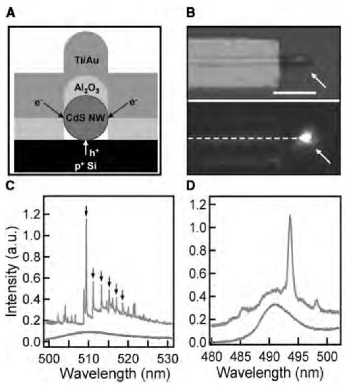
To enable more uniform injection, we have implemented a hybrid structure (Fig. 20A) in which holes are injected along the length of a CdS NW cavity from a p-Si electrode defined in a heavily doped p-Si layer on a planar substrate. Images of the room-temperature EL produced in forward bias from these structures (Fig. 20B) show strong emission from the exposed CdS NW end. At low injection currents, the spectrum of the end emission (Fig. 20C) shows a broad peak with FWHM — 18 nm. Significantly, when the injection current is increased further, we found that the emission intensity increased abruptly, and the spectrum quickly collapsed into a limited number of very sharp peaks with a dominant emission line at 509.6 nm (Fig. 20C). The sharp peaks of this device had an average spacing of ca. 1.8 nm, which is consistent with the Fabry-Perot cavity modes for the length of the NW device. Other small, sharp peaks are also observed and their explanation will require more detailed consideration of the NW cavity. Further more, low-temperature measurements (7 K) made on independent CdS injection laser devices. (Fig. 20D) show clearly that the spontaneous emission spectrum can collapse to a single mode, and moreover, these results are very similar to the low-temperature optically pumped results, and thus unambiguously demonstrate the formation of injection NW laser.
Using individual NWs as the laser cavity and gain medium for laser diodes represents a new and powerful approach for producing integrated electrically driven photonic devices. This basic approach, which relies upon bottom-up assembly of the key laser cavity/ medium in a single step, can be extended to other materials, such as GaN and InP NWs, to produce nanoscale lasers that not only cover the ultraviolet through near infrared spectral regions but also can be integrated as single or multicolor laser source arrays in silicon microelectronics and lab-on-a-chip devices. There are also scientific and technical challenges that may need to be addressed to realize this potential, including the development of more efficient cavities and injection schemes. Both issues could be addressed at the NW growth stage prior to device assembly by preparing Bragg gratings at the NW ends through axial composition modulation,[54] and using core-shell NW structure[61] to enable uniform injection into the active medium/cavity, respectively. By addressing these and other issues, such as quantifying contributions to optical losses within the NW cavity, NW lasers could be developed into systems that impact a number of areas where solid state lasers are used today, including telecommunications and data storage, and may enable new applications in highly integrated chemical/biological sensors, near-field optical lithography, a host of scanning probe microscopies, and perhaps even laser-based surgery with unprecedented resolution.
Fig. 20 Nanowire electrical injection laser. (A) Schematic showing the cross section of the device structure. (B) (Top) Optical image of a device described in (A). The arrow highlights the exposed CdS NW end. Scale bar, 5 mm. (Bottom) EL image recorded from this device at room temperature with an injection current of ca. 80 mA. The arrow highlights emission from the CdS NW end. The dashed line highlights the NW position. (C) Electroluminescence spectra obtained from the NW end with injection currents of 120 mA (lower curve) and 210 mA (upper curve). The black arrows highlight Fabry-Perot cavity modes with an average spacing of 1.83 nm. The green spectrum is shifted upward by 0.15 intensity units for clarity. (D) Emission spectra from a CdS NW device with injection currents of 200 mA (lower curve) and 280 mA (upper curve) recorded at 8 K. The spectra are offset by 0.10 intensity units for clarity.
