Logic XOR and half adder circuit
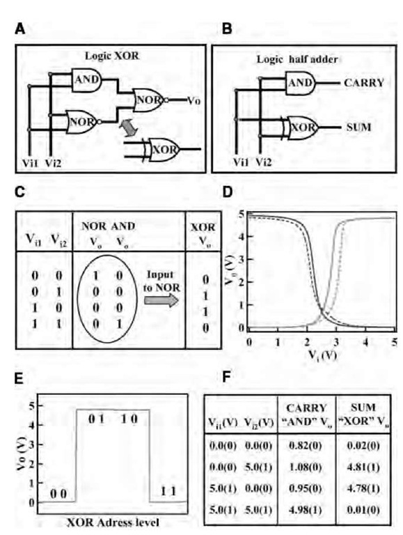
Logic OR, AND, and NOR (NOT) gates form a complete set of key logic elements and enable the organization of virtually any logic circuit. To demonstrate the potential for integration of such logic gates, we have interconnected multiple AND and NOR gates to implement basic computation in the form of an XOR gate (Fig. 31A), which corresponds to the binary logic function SUM, and a half adder (Fig. 31B), which corresponds to the addition of two binary bits. The XOR gate is configured by using the output from AND and NOR gates as the input to a second NOR gate, while the logic half adder uses an additional logic AND gate as the CARRY. The truth table for the XOR structure (Fig. 31C) confirms this logic operation. Significantly, the measured Vo—Vi transport data for the XOR device (Figs. 31D,E) show 1) that the output is logic-0 or low when the inputs are both low or high, and logic-1 or high when one input is low and the other is high, and 2) that the response is highly nonlinear. The linear response region corresponds to a voltage gain in excess of 10 and is typical of the devices measured to date. We note that this large gain is achieved in an XOR configured from a low gain diode AND gate, and is due to the high gain of the cNW-FET NOR gate. These data are summarized in the experimental truth table (Fig. 31F), which demonstrates that the response is that of the binary logic SUM operation. Significantly, with another AND gate as CARRY, a logic HALF ADDER is formed and can be used to carry out calculations in a manner similar to conventional electronics.
Fig. 31 Logic XOR gate and half adder. (A) Schematic of logic XOR gate constructed using the output from an AND and NOR as the input to a second NOR gate. (B) Schematic for logic half adder. (C) Truth table for logic XOR gate. (D) XOR output voltage vs. input voltages. The slope of the Vo—Vi data shows that the gain exceeds 10. The XOR gate was achieved by connecting the output electrodes of an AND and NOR gate to two inputs of another NOR gate. (E) The output voltage vs. the four possible logic address level inputs for the XOR gate. (F) Experimental truth table for the logic half adder. The logic half adder was obtained by using the XOR gate as the SUM and an AND gate as the CARRY.
Summary and Future Directions
In this section, we have demonstrated clearly that our ability to synthesize rationally NWs with controlled electronic properties, to configure them into individual functional NW devices, and to assemble NWs into regular arrays enables the bottom-up approach to move to new levels, including the assembly of devices with an unprecedented level of reproducibility, the integration of these device elements into complex diode and transistor logic gates without resorting to conventional lithography, and the interconnection of logic gates to carry out basic digital computation.
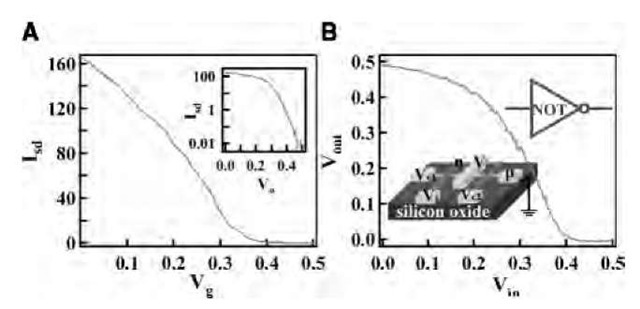
We also note that the OR and AND diode logic gates do not exhibit voltage gain; however, OR and AND logic with substantial gain could be realized if implemented using cNW-FETs. For example, logic OR can be achieved with the NOR gate by reversing the bias and ground connections to the p-Si NW. The AND function could also be implemented using cNW-FETs in parallel (vs. series for OR). In addition, due to finite turn-on voltage of the p-n diodes used in our diode-based OR/AND gates, the overall logic circuits were typically operated at relatively high voltage (5 V). Significantly, it is possible to operate at much lower voltage when all of the logic elements are implemented using cNW-FETs. For example, a logic NOT gate operating at 0.5 V and exhibiting a voltage gain as high as 3 (Fig. 32) was achieved using two cNW-FETs. Such a low operation voltage is a significant improvement over relative high voltage operation of carbon NT circuits (1.5 V) and current commercial circuits (1.2 V), and could be very significant for reducing the power/heat load in highly integrated nanoelectronics logic circuits. In addition, both p- and n-channel transistors could be readily assembled using NWs, and would enable further reduction in power dissipation.
Fig. 32 Low voltage nanoinverter (logic NOT). (A) I-Vg behavior of a cNW-FET with onset of —0.4 V. The inset shows that the conductance of the FET can be changed over two orders of magnitude with less than 0.1 V change in the NW gate. The transconductance is —500 nS at Vsd = 0.5 V. (B) Output-input (Vo—Vi) for a nanoinverter configured from two cNW-FETs. The inverter has an operation voltage of about 0.5 V.
The assembly of key logic gates and computation circuits represents a substantial advance compared to previous studies of NTs and molecular systems. First, the controllable electronic characteristics of the NW building blocks and reproducible properties of the devices assembled from these blocks contrasts the much lower control achieved to date with NTs. We believe that predictable and reproducible assembly of device elements and arrays is especially important for integration without resorting to extensive top-down lithography to connect to those few devices that function. Second, the use of crossed NW devices defines all nanoscale device metrics without resorting to top-down lithography. For example, the introduction of the new concept of a cNW-FET incorporates three intrinsic nanometer scale metrics (channel width, length, and gate dielectric thickness) into our devices, and thus can potentially enable the whole circuit architecture to be scaled down to the nanometer level in a straightforward way. This achievement and potential is in stark contrast to NT and molecular devices where the critical device dimension reported to date (length for NTs and area for molecules) have been determined by the same top-down lithography used in conventional electronics. Third, these distinct nanometer scale metrics, which are controlled by synthesis and subsequent assembly, lead to and can potentially lead to significantly improved device characteristics such as high gain, high speed, and low power dissipation, which are especially important to future highly integrated nanoelectronics circuits.
Overall, the predictable and reproducible bench-top assembly of nanoscale crossed p-n diode and cNW-FET elements and arrays reviewed in this section, which have enabled the demonstration of all critical logic gates and basic computation, represent a significant step towards integrated nanoelectronics built from primarily bottom-up vs. top-down approaches. Further improvements can be made by assembling NWs directly onto predefined metal electrode arrays[74] and by creating more highly integrated circuit elements by feeding the output from NW to NW. Implementing these approaches could eliminate the conventional lithography used to wire-up devices investigated to date. In addition, in a crossbar array with 5 nm diameter NWs, it may be possible to achieve device densities approaching 1012/cm2, which is off the present semiconductor road map for top-down manufacturing. To achieve this goal of bottom-up manufacturing in the future will require substantial work—for example, in developing much greater sophistication in assembly and further improving materials synthesis—but are well within the realm of our current understanding and thus suggest a particularly bright and promising future for this approach to integrated nanoelectronics.
APPLICATION OF NANOSCALE DEVICES IN CHEMICAL AND BIOLOGICAL SENSING
Underlying Principle
Developments in nanotechnology will not only lead to improved electronics and make quantum jumps in electronics miniaturization, but could also enable significant advances in medicine and healthcare, which benefit mankind as a whole. For example, nanoscale devices could open up fundamentally new ways to probe single molecule properties, and allow in vivo monitoring of diseases, such as cancer, which could lead to detection at the earliest and most treatable stage.
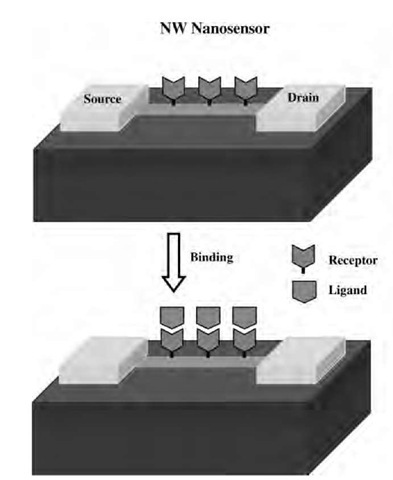
To this end, NW-based FETs have been exploited for highly sensitive and selective detection of chemical and biological species. Planar semiconductors have been used as the basis for many types of chemical and biological sensors in which detection can be monitored electrically and/or optically. For example, planar FETs can be configured as sensors by modifying the gate oxide with molecular receptors or a selective membrane for the analyte of interest.[76,77] Binding of a charged species then results in a depletion or accumulation of carriers within the transistor structures. An attractive feature of such chemically sensitive FETs is that binding can be monitored by a direct change in conductance or related electrical property, although the sensitivity and potential for integration are limited. Our nanoscale sensors are based on a similar framework using NW-based FETs (Fig. 33) but have some obvious advantages compared to planar semiconductor sensors. First, the large surface to volume ratio can dramatically increase the sensitivity. Binding of chemical or biological species to the surface of NWs can lead to depletion or accumulation of carriers in the "bulk” of nanometer diameter structures vs. only the surface region in a planar device, and increase the sensitivity to the single-molecule level. Second, high-density arrays of sensors could be readily prepared owing to the extremely small size of the NWs and the rational assembly techniques discussed in earlier sections of this review. Lastly, the small size of these nanosensors could enable minimally invasive in vivo sensors that could be readily coupled to other device functionality, such as telemetry and drug delivery systems. We have used Si NW-based FETs to demonstrate the principle and potential of such a nanoscale sensor approach.
Fig. 33 Underlying concepts for a nanosensor based on NW-FETs. A solid state NW-FET is transformed into a sensor by modifying the NW surface with molecular receptors. Binding of a charged species (ligand) then results in a depletion or accumulation of carriers within the transistor structures and changes the conductance of the NW-FET.
Chemical Sensors: The Case of pH
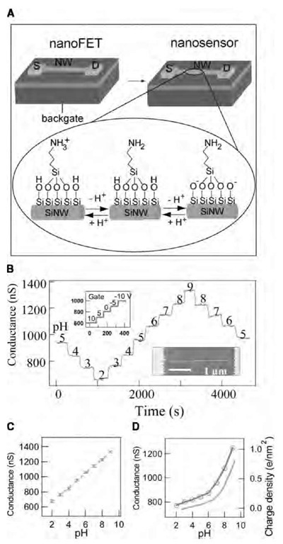
The underlying concept for the NW nanosensor can be illustrated in general for the case of pH sensor (Fig. 34).[78] Here, a Si NW solid state FET whose conductance is modulated by applied gate, is transformed into a nanosensor by modifying the silicon oxide surface with 3-aminopropyltriethoxysilane (APTES). The APTES provide a surface that can undergo protonation and deprotonation, where changes in surface charge (protonation) chemically gate the Si NW (Fig. 34A). The response of APTES-modified Si NWs to changes in solution pH (Fig. 34B) demonstrate that the NW conductance increases stepwise with discrete changes in pH from 2 to 9 and that the conductance is constant for a given pH. The changes in conductance are also reversible for increasing and/or decreasing pH. A typical plot of the conductance vs. pH (Fig 34C) shows that the pH dependence is linear over the pH 2-9 range and thus suggests that modified Si NWs could function as nanoscale pH sensors.
Fig. 34 NW pH detection. (A) Schematic illustrating the conversion of a NW-FET into a NW pH sensor. (B) Real-time reversible detection of the conductance changes of a modified Si NW as pH is changed from 2 to 9; the pH values are indicated on the conductance plot. Inset: (Top) Plot of the time-dependent conductance of a Si NW-FET as a function of the back-gate voltage. (Bottom) SEM image of a typical device. (C) Plot of the conductance vs. pH; the dashed line is linear fit through this data. (D) The conductance of an unmodified Si NW vs. pH. The dashed curve is a plot of the surface charge density for silica as a function of pH.
These results have been explained by considering the mixed surface functionality of the modified Si NWs. Covalently linking APTES to SiNW oxide surface results in a surface terminating in both -NH2 and -SiOH groups (Fig. 34A), which have different dissociation constants, pKa.[38,79] At low pH, the -NH2 group is protonated to -NH3+[79] and acts as a positive gate, which depletes hole carriers in the p-type SiNW and decreases the conductance. At high pH, -SiOH is deprotonated to -SiO—, which correspondingly causes an increase in conductance. The observed linear response can be attributed to an approximately linear change in the total surface charge density (vs. pH) because of the combined acid and base behavior of both surface groups. This point was supported with pH dependent measurements on unmodified (only -SiOH functionality) SiNWs, which showed a nonlinear pH dependence (Fig. 34D) similar to previous measurements of the pH dependent surface charge density of silica.[80]
Biological Sensors
The above results clearly demonstrate that NW-based FETs can be configured as chemical sensors. Since many biological molecules, such as proteins and DNA, are charged under physiological conditions, it is also possible to detect the binding of these macro-molecules to NW surfaces. We have demonstrated detection of biologically relevant species through the detection of proteins, antibodies, and metal ions.[78] These critical examples are reviewed briefly below.
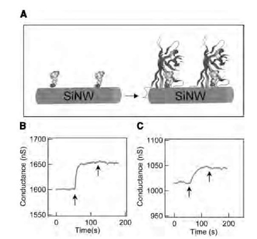
Initial investigations of protein detection by Si NW nanosensors were carried out for the well-characterized ligand-receptor binding of biotin-streptavidin (Fig. 35A) using biotin-modified NW surfaces.[78] Measurements showed that the conductance of biotin-modified Si NWs increased rapidly to a constant value upon addition of streptavidin solutions and that this conductance value was unchanged after the addition of pure buffer solution (Fig. 35B). The increase in conductance upon addition of streptavidin is consistent with binding of a negatively charged species to the p-type Si NW surface and the fact that streptavidin (pI — 5-6)[81] is negatively charged at the pH of these measurements. The absence of a conductance decrease with addition of pure buffer also agrees well with the small dissociation constant (Kd — 10—15 M) and correspondingly small dissociation rate of biotin- streptavidin.[81]
Fig. 35 Detection of protein binding. (A) Schematic illustrating a biotin-modified Si NW (left) and subsequent binding of streptavidin to the Si NW surface (right). The Si NW and streptavidin are drawn approximately to scale. (B) Plot of conductance vs. time for a biotin-modified Si NW, where first arrow corresponds to the addition of 250 nM strept-avidin, and the second arrow corresponds to the addition of pure buffer solution. (C) Conductance vs. time for a biotin-modified Si NW, where the two arrows have the same designation. The streptavidin solution had a concentration of 25 pM.
Significantly, the biotin-modified Si NWs nanosen-sors were also shown to exhibit very high sensitivity. Experiments indicate that it is possible to detect strep-tavidin binding down to a concentration at least as low as 10 pM (Fig. 35C). This detection level is substantially lower than the nanomolar range demonstrated recently by stochastic sensing of single molecules.[82] We note that a time-dependent increase in the conductance can be resolved immediately after streptavidin addition at very low concentrations, which reflects contributions from the forward binding rate and/or diffusion, although future studies will be required to resolve these contributions.
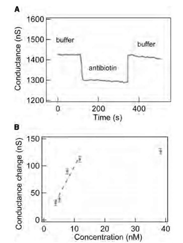
The above studies demonstrate that our NW nano-sensors are capable of highly sensitive and selective real-time detection of proteins, although the essentially irreversible biotin-streptavidin binding interaction precludes real-time monitoring of varying protein concentration. To explore this possibility, we studied the reversible binding of monoclonal antibiotin (m-antibiotin) to biotin.[83] Time-dependent conductance measurements made on biotin-modified Si NWs (Fig. 36A) exhibit a well-defined decrease after addition of m-antibiotin solution followed by an increase in the conductance to about the original value upon addition of pure buffer solution. The decrease in conductance upon m-antibiotin addition is consistent with the binding m-antibiotin, which was positively charged at the pH 7 of these experiments.[84] The time scale for the increase in conductance (seconds), which we associate with m-antibiotin dissociation, was also consistent with the reported dissociation rate constant.[83]
This reversible, real-time detection of m-antibiotin was further extended to monitor the Si NW sensor conductance as a function of m-antibiotin concentration in these studies.[78] These measurements showed a linear change in the conductance as a function of m-antibiotin concentration below —10 nm and saturation at higher values (Fig. 36B) and thus demonstrate several important facts. First, from the linear regime, we estimate that the dissociation constant, Kd, is of the order of 10—9 M, which is in good agreement with the value, —10—9M, determined previously.[84] Second, we can monitor protein concentration in real time, which could have important implications in basic research, for example, in monitoring protein expression, as well as in medical diagnostics. Lastly, preliminary experiments also suggest that the linear response dynamic range can be extended by applying a back gate to the NW, where gating can either increase or decrease the intrinsic binding constant.
Fig. 36 Real-time detection of reversible protein binding. (A) Plot of conductance vs. time for a biotin-modified Si NW, where ”antibiotin” corresponds to the addition of —3 mM m-antibiotin. (B) Plot of the conductance change of a biotin modified Si NW vs. m-antibiotin concentration; the dashed line is a linear fit to the four low concentration data points.
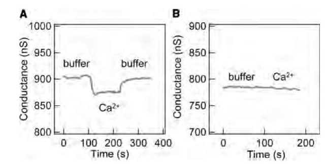
The concept of using NW-FETs modified with receptors or ligands for specific detection can be extended in many directions. For example, they can also be used to sense calcium ions (Ca2+), which are important for activating biological processes such as muscle contraction, protein secretion, cell death, and development.[85] To this end, a Ca2+ sensor was fabricated by immobilizing the calcium binding protein calmodulin onto Si NW surfaces. Conductance measurements made with such modified Si NW devices (Fig. 37) showed a drop in the conductance upon addition of a 25 mM Ca2+ solution, and a subsequent increase when a Ca2+-free buffer was subsequently flowed through the device. The observed conductance decrease is consistent with expected chemical gating by positive Ca2+, and the estimated dissociation constant, 10—5-10—6M, is in good agreement with the reported Kd for calmodulin.
Future Directions
The above studies demonstrate the potential of our NW nanosensors for highly sensitive and selective detection of chemical and biological species. Further development of this new type of nanosensors could also lead to antigen-antibody sensing and/or DNA detection. The availability of NWs with large gate responses should also enable detection down to the single molecule level. More generally, these nanosensors could enable many advances in both basic biological research, such as sensitive detection of many cellular species in real time in an array format to unravel complex signaling pathways, and biotechnology/medicine, where nanosensors might increase the speed of genome sequencing by many orders of magnitude and enable large scale studies designed to unravel the genetic contributions to complex diseases. Moreover, the ability to integrate these electrically monitored nanosensors with other components could facilitate development of multifunctional and minimally invasive implantable devices that enable detection and prevention of diseases at the earliest and most treatable stage.
Fig. 37 Real-time detection of Ca2+ ions. (A) Plot of conductance vs. time for a calmodulin-terminated Si NW, where ”Ca2+” corresponds to the addition of 25 mM Ca2+ solution. (B) Conductance vs. time for an unmodified Si NW.
SUMMARY AND PERSPECTIVES
In this topic, a brief survey of work drawn primarily from the authors’ laboratory has been presented. Overall, these examples illustrate a series key advances that should ultimately enable nanoelectronics fabrication and manufacturing from the bottom-up. First, we have developed a general approach for the synthesis of NW building blocks with well-controlled chemical compositions, physical dimensions, and electronic properties. Second, we have assembled a wide range of nanoscale electronic and optoelectronic devices from NW building blocks, and proposed and realized several conceptually new nanodevices, such as crossed NW p-n junctions and cNW-FETs, which are amenable for high-density integration. Third, we have developed methodologies to assemble NWs into integrated device arrays using microchannel fluidics or electrical fields, and have demonstrated integrated functional electronic circuits such as logic gates and carried out basic computations. Lastly, we have developed new types of nanosensors based on NW-FETs that can be used for highly sensitive and selective detection of chemical and biological species.
There is a very bright future for these electronically well-defined NW building blocks both in fundamental science and nanotechnologies. Specifically, we believe that only the very edge of a broad range of ideas has been touched, and that there remain many fascinating fundamental problems in these NW systems, such as the role of finite size and coherent states. Well-defined semiconductor NWs also represent exciting systems to probe fundamental questions about localization or delocalization of electrical carriers and optical excitons in 1D. Further investigations will be not only critical to understanding fundamental issues in 1D systems, but also central to improved device characteristics and possibly conceptually and fundamentally new type of devices, such as single photon emitters and detectors, which could be critical for future quantum communication and computation. Continuing efforts will be required to develop even better control of NW synthesis and more and more sophisticated assembly approaches that can vary device functionality over multilength scales. Lastly, developing new device concepts and integrated architectures will be increasingly essential as we move closer to ultrahigh density integrated nanosystems.
