Self-Propagating High-Temperature Synthesis
Self-propagating high-temperature synthesis (SHS) represents solid-state burning of reagents (metal and carbon for carbides or metal in nitrogen for nitrides) at a temperature of 2500 to 3000 K. Usually, the average size of grains in carbides produced by the SHS method is 5 to 20 mm.
A nanosized powder of titanium carbide was prepared by the SHS method using sodium chloride as an inert dilutant.[13] As titanium and carbon are burning, NaCl forms a melt, which insulates the formed carbide particles and prevents their growth. Also, NaCl dissolves well in water and can be easily separated from the synthesized carbide. The size of titanium carbide particles decreases with growing percentage of NaCl in the initial mixture. The average size of particles is about 100 nm.
Ordering in Nonstoichiometric Compounds as a Method of Producing a Nanostructure
A nanostructure in nonstoichiometric compounds such as MCy cubic carbides is produced through disorder-order transformations, which take place as phase transitions of the first kind with an abrupt change of the volume.[14] If a nonstoichiometric compound is cooled quickly from a high temperature, at which the disordered state is at equilibrium, ordering cannot be completed and the compound remains in a metastable disordered state. Because lattice constants of the disordered and ordered phases are different, stresses arise in the sample, leading to the cracking of crystallites at interfaces between the disordered and ordered phases and formation of a nanostructured powder.
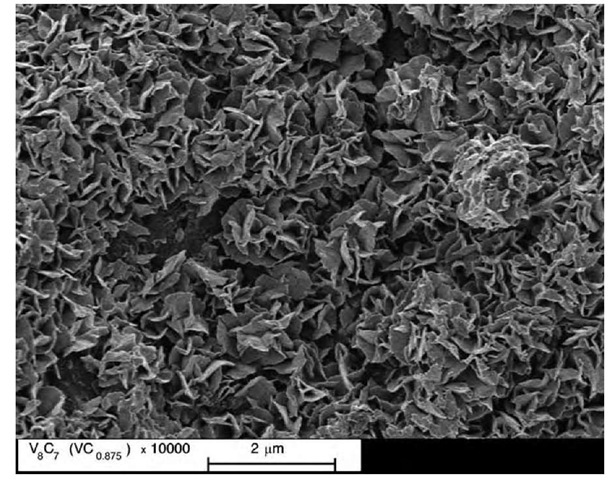
The first ordering-induced nanostructure was realized in a nonstoichiometric vanadium carbide.[15] The initial powder of the VC0 875 carbide with grains 1 to 2 mm in size was aged for a long time at 300 K. The aged powder contained agglomerates 5 to 30 mm in size, which were formed by particles measuring about 1 mm. The particles had a complicated structure (Fig. 7). Each entity ~ 1 mm in size looked like an open rosebud and contained a large number of nanocrystallites in the form of strongly bent plate disks 400 to 600 nm in diameter and 15 to 20 nm thick (Fig. 8). The bulk of the nano-crystallites consisted of the V8C7-ordered carbide, while the surface layer about 0.7 nm thick included a great number of vacancy agglomerates.
PREPARATION OF BULK NANOCRYSTALLINE SUBSTANCES
Disorder-Order Transformations
A nanostructure may be produced not only by ordering of powders, but also bulk nonstoichiometric compounds. Bulk samples of the VC0.875 carbide were prepared using a hot pressing of a powder of disordered vanadium carbide at a temperature of 2000 K and a pressure of 2025 MPa.[16] The size of grains in sintered samples was 10 to 60 mm. The sintered samples were annealed at 1370 K for 2 hr and then were cooled slowly (at a rate of 100 K hr-to 300 K or quenched from 1500 to 300 K. The maximum thermal treatment temperature approached the disorder-order transformation temperature Ttrans and was equal to Ttjans±100 K. Along with structural reflections, additional weak reflections corresponding to the V8C7-ordered phase appeared in the X-ray diffraction spectrum after both annealing and quenching.
Fig. 7 Microstructure of a powder of the VC0.875 vanadium carbide after long-term aging at ambient temperature in an ambient atmosphere (x 10000 magnification).
Fig. 8 Morphology of particles of an aged powder of the VC0.875 carbide ( x 50000 magnification). (From Refs. [15,16].) Particles about 1 mm in size represent a set of nanocrystallites having the shape of bent plate disks 400 to 600 nm in diameter and about 15-20 nm thick.
The V8C7-ordered phase was formed thanks to the disorder-order transformation. The grain size of the basic phase did not change upon ordering, but superstructural lines widened because of a small size of domains of the ordered phase. Superstructural reflections widened most for the sample, which was quenched from 1500 K. This means that domains of the ordered phase were smallest in that sample. The size of domains was about 130 nm in annealed samples and ~ 20 nm in samples quenched from 1500 K.
Thus the nanostructure in the bulk nonstoichiometric vanadium carbide represented a set of domains of an ordered phase and was formed thanks to the VC0 875 ! V8C7 disorder-order phase transformation.
Ordering is an efficient method for creation of a nano-structure in bulk and powder nonstoichiometric compounds. Disorder-order transformations, which are accompanied by changes of the volume, can be used to produce a nanostructure not only in nonstoichiometric compounds, but also in substitutional solid solutions, including alloys.
Compaction of Nanopowders
A method for production of bulk nanocrystalline substances, which was proposed by researchers[17] in 19811986, has been well known. This technology uses the method of evaporation and condensation for production of nanoparticles, which are deposited on the cold surface of a rotating cylinder. Evaporation and condensation are realized in a rarefied inert gas, mostly helium. Particles of the surface condensate are usually faceted. The deposited condensate is removed from the cylinder surface using a special scraper and is placed in a collector. The inert gas is pumped out and the nanocrystalline powder is compacted in a vacuum first at a pressure of ~ 1 GPa and finally at a pressure up to 10 GPa. Bulk nanomaterials prepared by this method contain particles of an average size D from 1-2 to 80-100 nm and have a relative density of 85-97% depending on evaporation and condensation conditions. The absence of contact with the ambient atmosphere during synthesis and compaction of the nano-powder precludes contamination of the bulk samples. For production of bulk nanocrystalline oxides and nitrides,the metal is evaporated to an oxygen- or nitrogen-containing atmosphere.
Porosity of nanoceramics prepared by compaction of powders is connected with triple junctions of crystallites. It may be decreased and made more uniform by compaction of nanopowders and their sintering at relatively low temperatures T< 0.5Tm (Tm being the melting point).
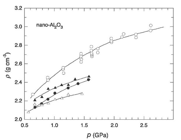
The magnetic pulsed method[18] is reduced to intensive dry pressing of powders. Pulsed compression waves cause vigorous heating of the powder thanks to the quick release of energy during friction of particles. When the size of particles is small (D < 0.3 mm), their heating time is shorter than the characteristic length of pulsed compression waves (1-10 msec). If compression wave parameters are chosen properly, it is possible to realize dynamic hot pressing of nanopowders thanks to their high surface energy. The magnetic pulsed method provides denser samples than steady-state pressing at nearly equal pressures (Fig. 9). Short-time heating reduces recrystallization caused by high temperatures and helps preserving a small size of particles.
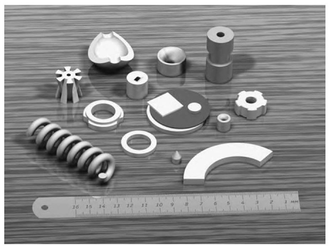
A promising method for compaction of ceramic nanopowders without plasticizers is dry cold ultrasonic pressing.[19] Ultrasound decreases interparticle friction, breaks agglomerates and coarse particles, and improves the volume distribution of particles. Therefore the density of the compact is enhanced, the growth of grains during sintering is limited, and the nanostructure is preserved. Ultrasonic pressing of nanopowders is especially efficient in the production of intricate articles, such as bushes, gear wheels, and spirals (Fig. 10).
Ceramic nanomaterials are sintered using heating with millimeter-range superhigh frequency (SHF) radiation.[20] Volume absorption of the SHF energy ensures one-time uniform heating of the whole sample and provides sintered ceramics having a homogeneous microstructure. The sintering temperature is 1300 to 2300 K. Microwave sintering of compacts, which had a relative density of 7080% and were made of a TiO2 nanopowder with an average size of particles equal to 20-30 nm, allowed producing sinters having a relative density of 97-99% and grains 200 to 220 nm in size on the average.
The existing methods for compaction of nanopowders and sintering of bulk nanomaterials already provide high-density intricate articles. However, it has been so far impossible to maintain the same small size of grains in sintered nanomaterials as in initial nanopowders. To keep the size of grains small, one has to decrease the temperature and duration of sintering and perform the sintering operation under a high pressure.
Film and Coating Deposition
Deposition on a cold or heated surface of a substrate allows making films and coatings, i.e., continuous layers of a nanocrystalline substance not more than several micrometers thick. Films may have different compositions and the size of their crystallites may change over a wide interval including the amorphous state and multilayer structures (superlattices). Pressing is not necessary because a bulk layer of a nanomaterial is obtained.
Fig. 9 Pressure dependence of the density p of the nanocrystalline oxide n-Al2O3 for steady-state and magnetic pulsed pressing: (1), (2), (3) represent steady-state pressing at temperatures of 300, 620, and 720 K, respectively; (4) represents magnetic pulsed pressing.
Deposition on a substrate may be realized from vapors, plasma, or a colloid solution. In the case of vapor deposition, a metal is evaporated in a vacuum or an oxygen- or nitrogen-containing atmosphere and then vapors of the metal or its compound (an oxide or a nitride) are condensed on a substrate. The size of crystallites in the film may be adjusted by varying the evaporation rate and the substrate temperature. Nanostructured films may be produced by deposition from plasma.
Oxide and sulfide semiconductor films are obtained by deposition on a substrate from colloid solutions. Nano-structured films containing nanoparticles of different semiconductors are prepared by the codeposition method. The methods of chemical and physical deposition from a gaseous phase (CVD and PVD) are traditionally used for producing of films.
Fig. 10 Ceramic articles synthesized by ultrasonic pressing of nanopowders.
Nanocrystallization of Amorphous Alloys
Nonporous nanostructured materials are produced by crystallization of amorphous metal alloys. Thin bands of amorphous alloys are made by melt spinning, i.e., quick (at a rate > 106K sec ) cooling of the melt on the surface of a rotating disk. Then the amorphous band is annealed to create a nanostructure.
Considerable study currently devoted to crystallization of amorphous alloys in connection with development of soft magnetic materials in Fe-Cu-M-Si-B (M=Nb, Ta, W, Mo, or Zr) systems.[21] Amorphous alloys of the Fe-Cu-Nb-Si-B system proved to be most successful. Their crystallization at 700-900 K resulted in formation of a uniform nanocrystalline structure. Grains of the a-Fe(Si) phase ~ 10 nm in size and copper clusters about 1 nm in size were uniformly distributed in the amorphous matrix of the alloy.
Crystallization of quickly solidifying amorphous alloys of the Al-Cr-Ce-M (M=Fe, Co, Ni, or Cu) system, which contained over 92 at.% Al, led to formation of a structure including an amorphous phase and Al-rich icosahedral nanoparticles (D ~ 5-12 nm) precipitated in the amorphous phase.[22] Alloys with this structure possess a high tensile strength (up to 1340 MPa), which approaches the strength of special steels.
Severe Plastic Deformation
Severe plastic deformation applies mostly to plastically deformable materials. In addition to the decrease in the average size of grains to 100-200 nm, it allows producing bulk samples with a nearly pore-free structure, which cannot be prepared by compaction of superfine powders.
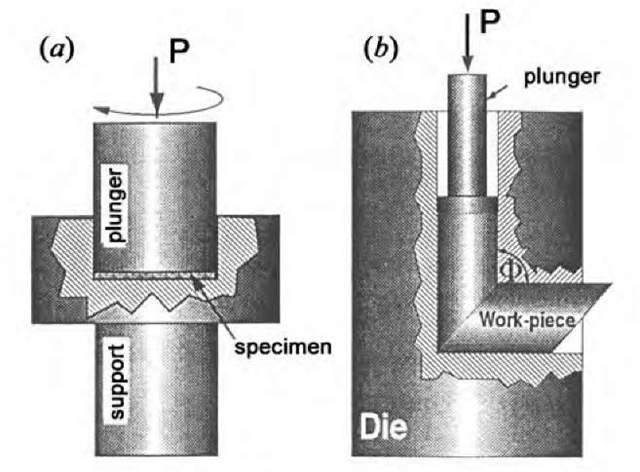
The main methods, which are used to considerably refine grains without breakage of samples, are high-pressure torsion and equal-channel angular (ECA) pressing (Fig. 11). The ECA pressing method was proposed in Ref. [23]. As compared with other methods of plastic deformation, this method provides the most uniform structure of substances. The structure and properties of submicrocrystalline materials, which were produced using severe plastic deformation, are described in Ref. [24].
The main feature of the structure of submicrocrystal-line materials prepared by deformation methods is nonequilibrium grain boundaries, which are a source of strong stresses. Triple junctions of grains represent one more source of stress. Annealing of submicrocrystalline materials causes changes in their microstructure. Initially, when the annealing temperature equals nearly one-third of the melting point, stresses are relaxed, grain boundaries acquire a more equilibrium state, and grains grow insignificantly. The further increase in the annealing temperature and time is followed by collective recrystal-lization, i.e., coarsening of grains.
Fig. 11 Schemes of main methods of severe plastic deformation:(a) high-pressure torsion; (b) equal-channel angular pressing.
The method of severe plastic deformation was used to produce a submicrocrystalline structure in such metals as Cu, Pd, Fe, Ni, and Co, aluminum, magnesium, and titanium alloys, and intermetallics. A bulk nanocrystalline sample with grains ~ 30-40 nm in size was prepared from a coarse (D ~ 2-5 mm) powder of a nonstoichiometric TiC0.62 titanium carbide by the method of high-pressure torsion.[8]
MICROSTRUCTURE OF BULK NANOCRYSTALLINE SUBSTANCES
In the simplest case, a nanocrystalline substance, which comprises atoms of one species, includes two components with different structures: grains (crystallites) 5 to 20 nm in size and intercrystalline boundaries up to 1.0 nm long. Crystallites have a similar structure and differ by their orientations and sizes only. The structure of interfaces is determined by the type of interatomic interactions and the mutual orientation of adjacent crystallites. It was thought originally that the intercrystalline substance is characterized by a random location of atoms and the absence of the long- and short-range order.[17] This state was called a gas-like structure, taking into account the location of atoms only.
Later studies showed that the atomic order on interfaces of nanosubstances approaches the atomic order in coarse-grain polycrystals. An example is a comparative study of the structures of coarse-grain palladium and nanocrystalline palladium n-Pd, which was prepared by evaporation and condensation. This study demonstrated that widening of diffraction reflections for n-Pd was a result of a small size of crystallites and stresses in grains or on interfaces rather than the gas-like structure of the grain-boundary phase or a large number of vacancies in grains.[25] Pores were detected only at triple junctions and not on the entire length of the interfaces.[26] The atomic density on intercrystalline boundaries proved to be nearly equal to its counterpart in crystallites.
According to Ref. [27] the coordination number of the first coordination sphere in an as-prepared n-Pd sample was 5-6% smaller than in coarse-grain palladium. However, almost all atoms were located at lattice sites in n-Pd samples, which were aged at room temperature for several months.[28] It was found[27,28] that grain boundaries in an as-prepared bulk n-Pd sample were in the equilibrium state with a small short-range order. This state was unstable even at room temperature and the sample acquired a more ordered state during 120-150 days, while the size of crystallites increased from 12 to 25-80 nm.[29]
Interfaces in compacted nanocrystalline substances may contain three types of defects:[2] separate vacancies, vacancy agglomerates or nanovoids at triple junctions, and large voids instead of missing crystallites (Fig. 12).
The annihilation of positrons[2,30] is the most reliable up-to-date method used for the study of free volumes in nanocrystalline substances. It is sensitive to extremely small concentrations of defects in solids, namely, from 10- 6 to 10- 3 defects per atom. The capture of positrons by defects allows using the electron-positron annihilation for analysis of interfaces in nanosubstances.
Fig. 12 Two-dimensional schematic model of a nanocrystal-line material with microscopic free volumes as detected by positron lifetime spectroscopy: (From Ref. [2] ) vacancy-like free volumes (with positron lifetime tj) in the interface, nano-voids (agglomerates of about 10 vacancies) at the triple junction of crystallites (t2), and a large void (t3) of the size of missing crystallites.
When a positron emitted from a radioactive source gets into a solid, it quickly loses its velocity and energy, which drops to the value corresponding to the crystal temperature. Then the positron diffuses in the substance in the free (delocalized) state and annihilates from this state in the characteristic lifetime tf of about 100 psec. During the time tf, the positron may move a distance of about 100 nm in defectless solids. Because the size of grains in a nanosubstance is smaller than the length of the positron diffusion in a defect-free grain, virtually all positrons may reach the grain surface and interfaces. If grains contain defects, which capture positrons, only part of positrons reach the grain boundary. Therefore it is possible to obtain information about intragrain defects. After a positron has been captured by a defect, it annihilates from the localized state in a time exceeding tf. The longer the lifetime of a positron in a defect is, the larger is the free volume.
Schaefer[2] and Wiirschum et al.[30] have given considerable study to nanomaterials by the electron-positron annihilation method. Vacancies and nanovoids were detected in nanocrystalline metals Al, Cu, Mo, Pd, Fe, and Ni, nanocrystalline silicon Si and zirconium oxide ZrO2, and many other materials. The investigations demonstrated that lifetime spectra of positrons usually contain two strong components and one weak component with intensities /j, l2, and l3=1 —l\—l2, which correspond to the lifetime tj, t2, and t3, respectively (Fig. 12). In nanocrystalline metals, the lifetime t1 approaches the lifetime of positrons t1V in lattice monovacancies of coarse-grain metals. Therefore tj is viewed as the lifetime of positrons in vacancy-like free volumes in grain interfaces (interface vacancies). The size of these vacancies corresponds to one or two missing atoms. The positron lifetime t2 characterizes annihilation of positrons in three-dimensional vacancy agglomerates (nanovoids) of the size of about 10 missing atoms. A very long lifetime t3 corresponds to annihilation of positrons in large voids of the size of missing crystallites.
Generally, the positron annihilation revealed the following: 1) the lifetime of positrons in nanocrystalline metals is longer than the lifetime tf of free delocalized positrons; 2) positrons are captured by monovacancies, vacancy complexes, and voids, whose size approaches the size of crystallites; and 3) free vacancy volumes, which capture positrons at low temperatures, belong to interfaces and not to crystallites.
The microstructure of submicrocrystalline substances, which are synthesized using severe plastic deformation, differs from the microstructure of compacted nanocrys-talline substances. The main feature of the structure of submicrocrystalline substances is the presence of randomly misoriented nonequilibrium grain boundaries.
Unannealed submicrocrystalline metals and alloys are characterized by extinction contours along grain boundaries, which point to large elastic stresses. Annealing eliminates dislocations from grains, extinction contours vanish, and a stripe contrast, which is typical of the equilibrium state, appears. The relaxation of interfaces is accompanied by growth of grains during annealing.

![Morphology of particles of an aged powder of the VC0.875 carbide ( x 50000 magnification). (From Refs. [15,16].) Particles about 1 mm in size represent a set of nanocrystallites having the shape of bent plate disks 400 to 600 nm in diameter and about 15-20 nm thick. Morphology of particles of an aged powder of the VC0.875 carbide ( x 50000 magnification). (From Refs. [15,16].) Particles about 1 mm in size represent a set of nanocrystallites having the shape of bent plate disks 400 to 600 nm in diameter and about 15-20 nm thick.](http://what-when-how.com/wp-content/uploads/2011/03/tmp28C192_thumb_thumb.jpg)


![Two-dimensional schematic model of a nanocrystal-line material with microscopic free volumes as detected by positron lifetime spectroscopy: (From Ref. [2] ) vacancy-like free volumes (with positron lifetime tj) in the interface, nano-voids (agglomerates of about 10 vacancies) at the triple junction of crystallites (t2), and a large void (t3) of the size of missing crystallites. Two-dimensional schematic model of a nanocrystal-line material with microscopic free volumes as detected by positron lifetime spectroscopy: (From Ref. [2] ) vacancy-like free volumes (with positron lifetime tj) in the interface, nano-voids (agglomerates of about 10 vacancies) at the triple junction of crystallites (t2), and a large void (t3) of the size of missing crystallites.](http://what-when-how.com/wp-content/uploads/2011/03/tmp28C196_thumb_thumb.jpg)
