Following the structural relaxation of the CNTs, the transmission and conductance were computed using the recursive Green’s function formalism.[11,78] A nearest-neighbor sp3 tight-binding Hamiltonian in a nonorthog-onal basis was chosen, and ideal semiinfinite contacts assumed at both ends. The parameterization scheme explicitly accounts for the effects of strain in the system through a bond length dependence of the Hamiltonian and the overlap matrices H and Sy.-.[79] First, the retarded Green’s function GR of the whole CNT was determined by solving the following equation:
where SL R are the retarded self-energies of the left and the right semiinfinite contacts. The transmission at each energy was then obtained[80] from the equation:
and right leads. Finally, the total conductance of the tube was computed by using Landauer-Buttiker formula:
where fo(E) is the Fermi-Dirac function. In Eqs. (3) and (4), summation over the repeating roman indices is implied. The lower and upper indices denote the covariant and contravariant components of a tensor.
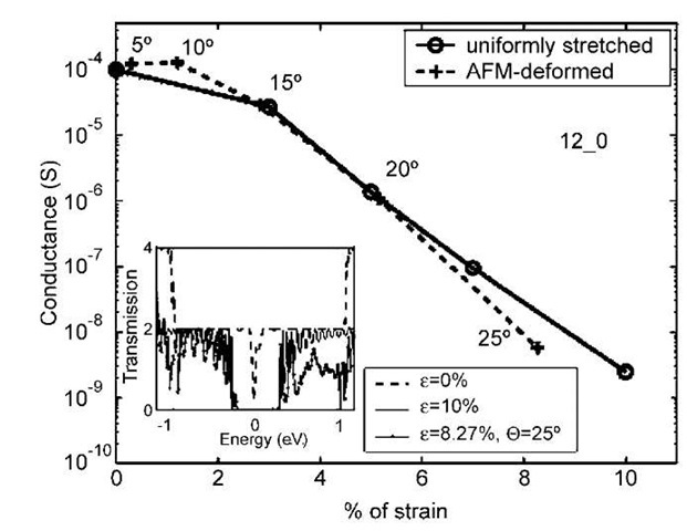
The simulations (Fig. 5) indicate that the conductance remains essentially constant for the (6,6) armchair tube up to deformation as large as 25°. However, for the (12,0) zigzag tube, the conductance drops significantly, by 2 orders of magnitude at 20° and 4 orders of magnitude at 8=25°. Because sp3 coordination could be ruled out, what could be the cause for such a large conductance drop in the experiment of Ref. [50] as well as for the metallic zigzag tube in Fig. 5? Also, why did the armchair tube display no significant drop in conductance even up to large angles of deformation?
A simple explanation emerges if one zooms out from the middle of the tube and looks at the profile of the whole tube under AFM deformation. One immediately discovers an overall stretching of the tube under AFM deformation, as indicated schematically in Fig. 6. Fig. 7 compares drop in conductance in the (12,0) tube subjected to: 1) AFM deformation; and 2) uniform stretching. Such comparison makes it clear that tensile strain is the main reason behind the conductance drop in an AFM-deformed metallic zigzag tube. It was also verified that the (6,6) armchair tube does not undergo any significant conductance drop upon stretching.[81]
To explain the differences in conductance drops of the armchair (6,6) and the zigzag (12,0) tubes as a function of strain, it helps to revisit the literature where a considerable amount of theoretical work already exists.[82-86] An important result[86] is that the rate of change of bandgap as a function of strain depends on the CNT chiral angle 0, more precisely as proportional to cos(30). Thus stretched armchair tubes (0=30°) do not open any bandgap, and always remain metallic. On the other hand, a metallic (3n,0) zigzag tube (0=0) can open a bandgap of ~ 100 meV when stretched by only 1%. This bandgap increases linearly with strain, thus transforming the CNT into a semiconductor at a strain of only a few percent. In general, all metallic tubes with n1 – n2=3n will undergo the above metal-to-semiconductor transition, the effect being the most pronounced in metallic zigzag tubes. An experiment such as that in Ref. [50] is thus expected to show a decrease in conductance upon AFM deformation for all CNTs except the armchair tubes. Researchers are also beginning to explore the electromechanical response of a squashed CNT,[87,88] where sp3 coordination is a possibility.
Fig. 7 Conductance of an AFM tip-deformed (12,0) tube compared to the same tube under a uniform stretch. Actual angles of tip deformation are indicated. The % strain for the AFM-deformed tube is computed from the average C—C bond stretch in the middle of the straight portion of the tube. The inset shows transmission in the vicinity of the Fermi surface (energy = 0) for a uniform strain of 10% and a tip-deformation angle of 25°, compared to the nondeformed tube.
In addition to the above results for metallic CNTs, theory also predicts that for semiconducting tubes (n1 -n2 ^ 3n), the bandgap can either increase (for n1 -n2 = 3n— 2) or decrease (for n1 -n2=3n— 1) with strain. These results have recently prompted more detailed experiments on a set of metallic and semiconducting CNTs deformed with an AFM tip,[89] as well as on CNTs under experimental tensile stretch.[90] Commercial applications from such work could lead to novel pressure sensors, transducers, amplifiers, and logic devices.[91]
NANOWIRES AND NANORIBBONS
In spite of tremendous advances in carbon nanotube research, there remain a number of practical difficulties hindering many applications. Cheap mass production remains one of the biggest hurdles. Other technological challenges involve controlling CNT chirality, isolating/ separating CNTs from bundles, alignment in nano-composites, and so on. Chemical insertness of the CNT poses big problems in functionalization, sensor applications, and adhesion to structural materials. The above deficiencies have prompted researchers to explore other types of one-dimensional nanostructures. These efforts have recently led to the synthesis of nanowires and nanoribbons. Nanowires are typically solid (i.e., not hollow) cylindrical objects with a nearly uniform diameter of a few tens of nanometers or less. So far, most nano-wires[1] have been synthesized from standard semiconductors: Si, Ge, GaAs, GaP, GaN, InAs, InP, ZnS, ZnSe, CdS, CdSe, and mixed compounds. Semiconducting nanowires have great potential in electronic and optoelectronic applications at the nanoscale. In addition, conducting nanowires made of transition and noble metals, silicides (ErSi2), and polymeric materials have also been investigated in connection with interconnect applications.
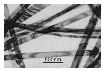
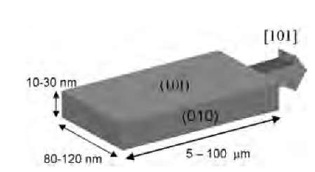
Nanoribbons are a close cousin of the nanowires. As the name suggests, they possess a uniform rectangular cross-section with well-defined crystal structure, exposed planes, and growth direction (Figs. 8 and 9). So far, nanoribbons have primarily been synthesized from the oxides of metals and semiconductors. In particular, SnO2 and ZnO[92-94] nanoribbons have been materials systems of great current interest because of their potential applications as catalysts, in optoelectronic devices, and as chemical sensors for pollutant gas species and biomole-cules.[95-97] Although they grow to tens of microns long, the nanoribbons are remarkably single-crystalline and essentially free of dislocations. Thus they provide an ideal model for the systematic study of electrical, thermal, optical, and transport processes in one-dimensional semiconducting nanostructures, and their response to various external process conditions.
Fig. 8 TEM bright-field image of SnO2 nanoribbons displaying strain contrast induced by bending of the ribbons. Each nanoribbon is single-crystalline without any dislocations.
SnO2 Nanoribbons: A Brief Introduction
SnO2 nanoribbons are usually synthesized by evaporating SnO or SnO2 powder at high temperature, followed by deposition on an alumina substrate in the downstream of an Ar gas flow.[92] Field-emission scanning electron microscopy (FE-SEM) and transmission electron microscopy (TEM) revealed that the ribbons: 1) possess a highly crystalline rutile structure; 2) grow tens of microns long in the (101) direction; 3) display a uniform quasirectangular cross-section perpendicular to the growth direction; and 4) present the (101) and (010) rutile planes as surface facets along the growth axis, with dimensions ranging from 80 to 120 nm by 10 to 30 nm (Fig. 9). Rutile SnO2 is a wide bandgap (3.6 eV) n-doped semiconductor, with the intrinsic carrier density determined by the deviation from stoichiometry, primarily in the form of oxygen vacancies.[98]
Fig. 9 Schematic diagram of a SnO2 nanoribbon, showing typical dimensions, exposed planes, and growth direction.
Fig. 10 Simulation supercells representing exposed surfaces of a SnO2 nanoribbon: (a) (101) surface; (b) (010) surface. Surface atoms are shown in ball representation. White (larger) balls and black (smaller) balls represent Sn and O atoms, respectively. Sn1 and Sn2 are neighboring Sn atoms connected with a bridging O.
SnO2 Nanoribbons as Chemical Sensors
Recent experiments with SnO2 nanoribbons[99] indicate that these are highly effective in detecting even very small amounts of harmful gases such as NO2. Upon adsorption of these gases, the electrical conductance of the sample decreases by more than 1 order of magnitude. More interestingly, it is possible to remove the adsorbates by shining UV light, and the electrical conductance is completely restored to its original value. Such single-crystalline sensing elements have several advantages over conventional thin-film oxide sensors: low operating temperatures, no ill-defined coarse grain boundaries, and high active surface-to-volume ratio.
Electron-withdrawing groups such as NO2 and O2 are expected to deplete the conduction electron population in the nanoribbon, thereby leading to a decrease in electrical conductance. To investigate this, first-principles DFT calculations of the adsorption process of NO2, O2, and CO on the exposed (101) and (010) surfaces, as well as the edge atoms of a SnO2 nanoribbon, were carried out. The DFT code used was DMol3,[62,63,71-73] with the same basis set, parameter settings, and exchange-correlation functional as in the section ”Atomic and Electronic Structure.” Nanoribbon surfaces were represented in periodic supercells (Figs. 10 and 11), and accurate Brillouin zone integration was performed by careful sampling of k-points chosen according to the Monkhorst-Pack scheme,[100] with a k-point spacing of 0.1 A_ V To estimate charge transfer to adatoms, the partial charge on each atom was computed by using the Mulliken population analysis.[101]
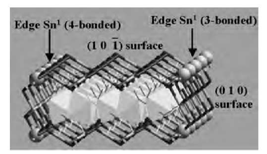
In bulk rutile SnO2, the Sn atoms are octahedrally coordinated with six O neighbors, while each O atom is a threefold bridge between neighboring Sn centers. At both (101) and (010) surfaces, the Sn atoms lose an O neighbor,thereby becoming fivefold coordinated (Fig. 10a,b). The surface O atoms become twofold-coordinated bridges connecting neighboring surface Sn atoms (Fig. 10a,b). Both surfaces were represented by three layers of Sn, each layer being sandwiched between two O layers. The bottom SnO2 layer was fixed to simulate the presence of several bulk-like layers in the actual sample. To reduce interaction with periodic images, the surface unit cell was doubled in the direction of the smaller surface lattice constant, and a vacuum of 15 A was placed normal to the surface. To simulate nanoribbon edges [i.e., lines of intersection of (101) and (010) planes], a structure similar to that in Fig. 11 was embedded in a periodic supercell with the smallest repeat period (5.71 A) along the length of the ribbon, and a vacuum of 15 A normal to both the (101) surface (y-axis) and the (010) surface (x-axis). At the nanoribbon edges, the Sn atoms can be either threefold- or fourfold-coordinated (Fig. 11).
Fig. 11 Simulation supercells representing SnO2 nanoribbon edges. For clarity, the periodic cell is not shown, and the interior atoms are represented by polyhedra. The edge (Sn) atoms are shown in ball representation.
Details of the results on binding energy and charge transfer are discussed elsewhere.[102] Important results are summarized below:
1. All adsorbate structures involve one or more bonds to surface Sn atoms. The binding energy on different surfaces and edges increases in the sequence (010)<(101) <3-fold edge<4-fold edge.
2. NO2 adsorption displays a very rich chemistry because it can either form a single bond to a surface Sn, or can adsorb in the bidented form through two single bonds to neighboring Sn atoms. The doubly bonded NO2 is 2-3 kcal/mol more stable than the single-bonded NO2, and the binding energies are in general 4-5 kcal/mol higher on the (101) surface than on the (010). Activation barrier between the doubly bonded and single-bonded structures is expected to be low, which should make the NO2 species mobile on the exposed faces by performing a series of random walk steps along well-defined rows of Sn atoms on the surface.
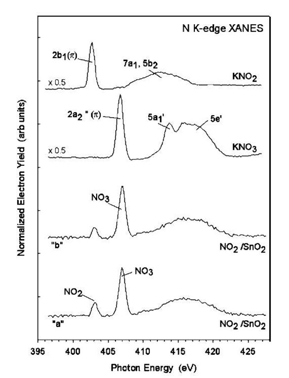
3. When two NO2 molecules meet on the surface, either through random walk as described above, or through the incidence of a second NO2 from the gas phase in the vicinity of an already chemisorbed NO2, there is a transfer of an O atom from one NO2 to the other, thus converting it to a surface NO3 species. The net dis-proportionation reaction NO2+NO2! NO3+NO is well known in chemistry. The bidented NO3 group has a substantially higher binding energy, especially on the (101) surface, and should not, therefore, be mobile. The resulting NO species is only weakly bound to the surface and should desorb easily. Synchrotron measurements using X-ray absorption near-edge spectroscopy (XANES) have recently confirmed the abundance of NO3 species on the nanoribbon surface following NO2 adsorption (Fig. 12).[102]
4. A CO likes to adsorb in the following manner: the C forms two single bonds to the surface—one with a surface Sn and another with a bridging O, while the O of the CO forms a double bond to the C and sticks out of the surface. This way, the C atoms attains its preferred 4-valency and the O has its bivalency satisfied.
Fig. 12 N K-edge XANES spectra acquired after exposing nanoribbons of SnO2 to NO2 at 300 K. Traces ”a” and ”b” correspond to two different nanoribbon samples, respectively. Included in the figure are the corresponding spectra for KNO2 and KNO3. (The assignment of the features in these spectra is discussed in Refs.
5. On a defect-free surface (i.e., surface with no O vacancies), the O2 molecules can only weakly physisorb. In this configuration, there is no charge transfer to the O2, and therefore a nanoribbon surface without surface O vacancies should be insensitive to atmospheric oxygen. However, at surface O-vacancy sites, the O2 molecule has a strongly bound chemisorbed structure in the form of a peroxide bridge.
6. Both NO3 groups and chemisorbed O2 (at O-vacancy sites) accept significant amount of electronic charge from the surface. Therefore such adsorbates should lead to the lowering of electrical conductance of the sample. On the other hand, CO donates a moderate amount of electrons to the surface, and is therefore expected to increase the electrical conductance. All these results are consistent with direct experimental measurements of sample conductance.[96,99,105] Charge transfer between molecular species (donor or acceptor alike) and the nanoribbon surface could thus serve as a general mechanism for ultrasensitive chemical and biological sensing by using single-crystalline semiconductor nanowires.


