Digital Signals—Pulse Code Modulation
In most applications that employ optical time-division multiplexing, signals are usually sent in a pulse-code-modulated format, as opposed to sending optical samples that are directly proportional to the analog signal amplitude (e.g., PAM, PPM, and PLM). The key feature of sending the information in the form of a digital code is that the analog form of the signal can be corrupted with noise that generally cannot be separated from the signal. The pulse code modulation format provides a mechanism by which the digitization and quantization, or coding, of the signal produces a signal that can be recovered from the noise introduced by the communication link.
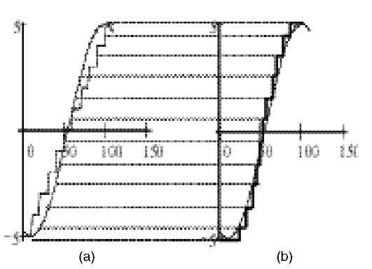
The limitation of a simple analog communication system is that once noise is introduced onto the signal, it is impossible to remove. When quantization is employed, a new signal is created that is an approximation of the original signal. The main benefit of employing a quantization technique is that, in large part, the noise can be removed from the signal. The main characteristic of a general quantizer is it has an input-output characteristic that is in the form of a staircase, as shown in Fig. 6. It is observed that while the input signal Vin(t) varies smoothly, the output Vo(t) is held constant at a fixed level until the signal varies by an amount of Vmax/N,where N is the number of levels by which the output signal changes its output level. The output quantized signal represents the sampled waveform, assuming that the quantizer is linearly related to the input. The transition between one level and the next occurs at the instant when the signal is midway between two adjacent quantized levels. As a result, the quantized signal is an approximation of the original signal. The quality of the approximation may be improved by reducing the step size or increasing the number of quantized levels. With sufficiently small step size or number of quantized levels, the distinction between the original signal and the quantized signal becomes insignificant. Now, consider that the signal is transmitted and subsequently received, with the addition of noise on the received signal. If this signal is presented to the input of another identical quantizer, and if the peak value of the noise signal is less than half the step size of the quantizer, the output of the second quantizer is identical to the original transmitted quantized signal, without the noise that was added by the transmission channel! It should be noted that this example is presented only to illustrate the concept of noise removal via quantization techniques. In reality, there is always a finite probability—no matter how small—that the noise signal will have a value that is larger than half the step size, resulting in a detected error. While this example shows the benefits of quantization and digital transmission, the system trade-off is that additional bandwidth is required to transmit the coded signal.
FIGURE 6 The input-output "staircase" transfer function of a digital quantizer. (a) Staircase function and sinusoid. (b) The resultant quantized function superimposed on the original sinusoid, showing a slight deviation of the quantized signal from the original sinusoid.
It should be noted that the resultant quantized signal shown in Fig. 6 possesses a slight distortion that results from the quantization process. This slight distortion generates a signal-to-noise ratio (SNR) that is not uniform for all values of received signals. This nonuniform SNR tends to increase the error in the transmitted signal due to quantization. One method of reducing this quantization error is to predistort the signal such that small-amplitude signals are received with the same SNR as large-amplitude signals. This process of predistorting the signal is called compressing, and is achieved in devices called companders. Obviously, on the receiver end, a similar process to invert the predistortion process is required, and is accomplished in an expander.
Pulse Code Modulation
A signal that is to be quantized prior to transmission has been sampled as well. The quantization is used to reduce the effects of noise, and the sampling allows us to time-division multiplex a number of users. The combined signal-processing techniques of sampling and quantizing generate a waveform composed of pulses whose amplitudes are limited to a discrete number of levels. Instead of these quantized sample values being transmitted directly, each quantized level can be represented as a binary code, and the code can be sent instead of the actual value of the signal. The benefit is immediately recognized when considering the electronic circuitry and signal processing required at the receiver end. In the case of binary code transmission, the receiver only has to determine whether one of two signals was received (e.g., a 1 or a 0), as compared to a receiver system, which would need to discern the difference between the N distinct levels used to quantize the original signal. The process of converting the sampled values of the signal into a binary coded signal is generally referred to as encoding. Generally, the signal-processing operations of sampling and encoding are usually performed simultaneously, and as such, the entire process is referred to as analog-to-digital (A-to-D) conversion.
Analog-to-Digital Conversion
The sampled signal, as shown in Fig. 5, represents the actual values of the analog signal at the sampling instants. In a practical communication system or in a realistic measurement setup, the received or measured values can never be absolutely correct because of the noise introduced by the transmission channel or small inaccuracies impressed on the received data owing to the detection or measurement process. It turns out that it is sufficient to transmit and receive only the quantized values of the signal samples. The quantized values of sampled signals, represented to the nearest digit, may be represented in a binary form or in any coded form using only 1s and 0s. For example, sampled values between 2.5 and 3.4 would be represented by the quantized value of 3, and could be represented as 11, using two bits (in base 2 arithmetic). This method of representing a sampled analog signal, as noted earlier, is known as pulse code modulation. An error is introduced on the signal by this quantization process. The magnitude of this error is given by
where N is the number of levels determined by N = 2B, and B is the B-bit binary code—for example, B = 8 for eight-bit words representing 256 levels. Thus one can minimize the error by increasing the number of levels, which is achieved by reducing the step size in the quantization process. It is interesting to note that using only four bits (16 levels), a maximum error of 2.5 percent is achieved, while increasing the number of bits to eight (256 levels) gives a maximum error of 0.15 percent.
Optical Representation of Binary Digits and Line Coding
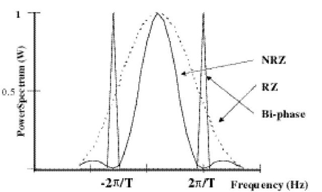
The binary digits can be represented and transmitted on an optical beam and passed through an optical fiber or transmitted in free space. The optical beam is modulated to form pulses to represent the sampled and digitized information. A family of four such representations is shown in Fig. 7. There are two particular forms of data transmission that are quite common in optical communications owing to the fact that their modulation formats occur naturally in both direct and externally modulated optical sources. These two formats are referred to as non-return-to-zero (NRZ) and return-to-zero (RZ). In addition to NRZ and RZ data formats, pulse-code-modulated data signals are transmitted in other codes that are designed to optimize the link performance, owing to channel constraints. Some important data transmission formats for optical time-division multiplexed networks are code mark inversion (CMI) and Manchester coding or bi-phase coding. In CMI, the coded data has no transitions for logical 1 levels. Instead, the logic level alternates between a high and low level. For logical 0, on the other hand, there is always a transition from low to high at the middle of the bit interval. This transition for every logical 0 bit ensures proper timing recovery. For Manchester coding, logic 1 is represented by a return-to-zero pulse with a 50 percent duty cycle over the bit period (a half-cycle square wave), and logic 0 is represented by a similar return-to-zero waveform of opposite phase, hence the name bi-phase. The salient feature of both bi-phase and CMI coding is that their power spectra have significant energy at the bit rate, owing to the guarantee of a significant number of transitions from logic 1 to 0. This should be compared to the power spectra of RZ and NRZ data, which are shown in Fig. 8. The NRZ spectrum has no energy at the bit rate, while the RZ power spectrum does have energy at the bit rate—but the RZ spectrum is also broad, having twice the width of the NRZ spectrum. The received data power spectrum is important for TDM transmission links, where a clock or synchronization signal is required at the receiver end to demultiplex the data. It is useful to be able to recover a clock or synchronization signal derived from the transmitted data, instead of using a portion of the channel bandwidth to send a clock signal. Therefore, choosing a transmission format with a large power spectral component at the transmitted bit rate provides an easy method of recovering a clock signal.
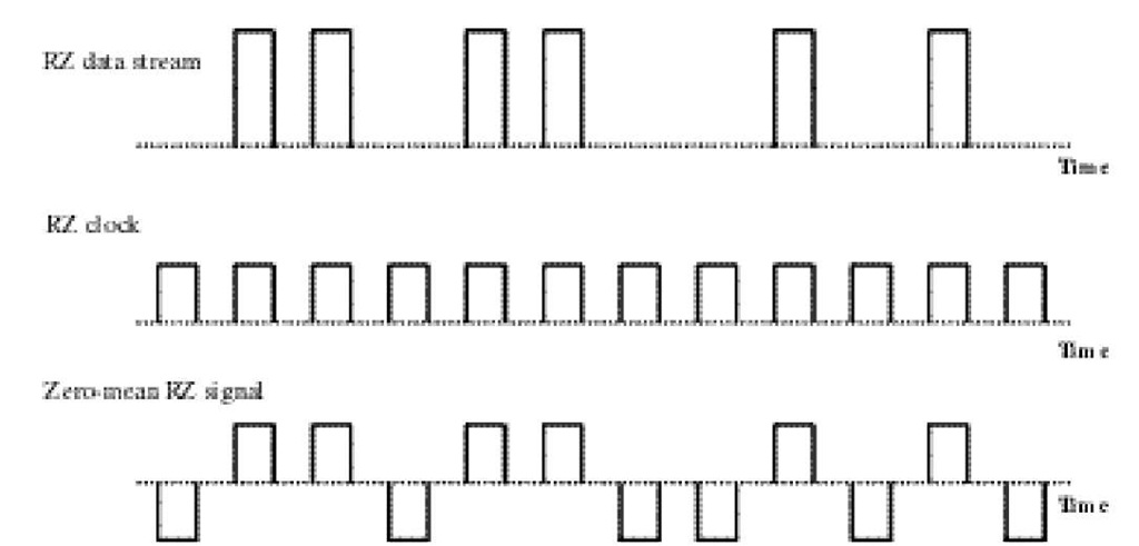
Consider for example the return-to-zero (RZ) format just discussed. If the transmitted bits are random independent 1s and 0s with equal probability, the transmitted waveform can be considered to be the sum of a periodic clock sequence with half of the amplitude and a random sequence with zero mean as shown in Fig. 9.
FIGURE 7 Line-coded representations of the pulse-code-modulated logic signal 10110010111. NRZ: non-return-to-zero format; RZ: return-to-zero format; bi-phase, also commonly referred to as Manchester coding; CMI: code mark inversion format.
FIGURE 8 Power spectra of NRZ, RZ, and bi-phase line coded data. Note the relative power at the bit rate.
The Fourier transform of the clock component has a peak at the bit frequency, and the Fourier transform of the random component is 0 at the bit frequency. Therefore, if there is a narrow-bandpass filter at the receiver with the received signal as the input, the clock component will pass through and the random part will be rejected. The output is thus a pure sinusoid oscillating at the clock frequency or bit rate. This concept of line filtering for clock recovery is schematically represented in Fig. 10.
Generally, pulse-code-modulated signals are transmitted in several different formats to fit within the constraints determined by the transmission channel (bandwidth and so on). It is clear from Fig. 8 that the power spectrum of return-to-zero PCM data has a spectral spread that is approximately twice that of non-return-to-zero PCM data.
FIGURE 9 Illustration showing a random RZ data stream, along with its RZ clock component and its zero-mean counterpart. Note that the zero-mean signal results from the difference between the RZ data and the clock component.
FIGURE 10 Principle of clock recovery using line filtering. (a) Input RZ data stream. (b) Filtered time-domain clock signal. (c) Schematic of an electrical tank circuit for realizing a bandpass filter. (d) Power spectrum of a periodic RZ sequence. (e) Power spectrum of the filtered signal.
Both formats have a large amount of power in the DC and low-frequency components of their power spectra. In contrast, the bi-phase code has very low power in the DC and low-frequency portion of the power spectrum, and as a result is a very useful format for efficient timing recovery.
Timing Recovery
Time-division multiplexing and time-division multiple-access networks inherently require timing signals to assist in demultiplexing individual signals from their multiplexed counterparts. One possible method is to utilize a portion of the communication bandwidth to transmit a timing signal. Technically, this is feasible; however (1) this approach requires hardware dedicated to timing functions distributed at each network node that performs multiplexing and demultiplexing functions, and (2) network planners want to optimize the channel bandwidth without resorting to dedicating a portion of the channel bandwidth to timing functions. The desired approach is to derive a timing signal directly from the transmitted data. This allows the production of the required timing signals for multiplexing and demultiplexing without the need to use valuable channel bandwidth.
As suggested by Fig. 10, a simple method for recovering a timing signal from transmitted return-to-zero data is to use a bandpass filter to pass a portion of the power spectrum of the transmitted data. The filtered output from the tank circuit is a pure sinusoid that provides the timing information. An important parameter to consider in line filtering is the quality factor, designated as the filter Q. Generally, the Q factor is defined as
where mo is the resonant frequency and Am is the bandwidth of the filter. It should also be noted that Q is a measure of the amount of energy stored in the bandpass filter, such that the output from the filter decays exponentially at a rate directly proportional to Q. In addition, for bandpass filters based on passive electrical circuits, the output peak signal is directly proportional to Q. These two important physical features of passive line filtering imply that the filter output will provide a large and stable timing signal if the Q factor is large. However, since Q is inversely proportional to the filter bandwidth, a large Q typically implies a small filter bandwidth. As a result, if the transmitter bit rate and the resonant frequency of the tank circuit do not coincide, the clock output could be zero. In addition, the clock output is very sensitive to the frequency offset between the transmitter and resonant frequency. Therefore, line filtering can provide a large and stable clock signal for large filter Q, but the same filter will not perform well when the bit rate of the received signal has a large frequency variation. In TDM bit timing recovery, the ability to recover the clock of an input signal over a wide frequency range is called frequency acquisition or locking range, and the ability to tolerate timing jitter and a long interval of zero transitions is called frequency tracking or hold over time. Therefore, the tradeoff exists between the locking range (low Q) and hold over time (large Q) in line filtering.
A second general scheme to realize timing recovery and overcome the drawbacks of line filtering using passive linear components is the use of a phase-locked loop (PLL) in conjunction with a voltage-controlled oscillator (VCO) (see Fig. 11a). In this case, two signals are fed into the mixer.
FIGURE 11 (a) Schematic diagram of a phase-locked loop using a mixer as a phase detector and a voltage-controlled oscillator to provide the clock signal that can track phase wander in the data stream. (b) Data format conversion between input NRZ data and RZ output data using an electronic logic gate. The subsequent RZ output is then suitable for use in a clock recovery device.
One signal is derived from the data (e.g., from a line filtered signal possessing energy at the bit rate), while the second signal is a sinusoid generated from the VCO. The mixer is used as a phase detector and produces a DC voltage that is applied to the VCO to adjust its frequency of operation. The overall function of the PLL is to adjust its own voltage to track the frequency and phase of the input data signal. Owing to the active components in the PLL, this approach for timing recovery can realize a broad locking range, low insertion loss, and good phase-tracking capabilities. It should be noted that while the concepts for timing recovery described in this section were illustrated using techniques that are not directly applicable to ultra-high-speed optical networking, the underlying principles will still hold for high-speed all-optical techniques. These approaches are discussed in more detail later in the topic.
While both these techniques require the input data to be in the return-to-zero format, many data transmission links use non-return-to-zero line coding owing to its bandwidth efficiency. Unfortunately, in the NRZ format there is no component in the power spectrum at the bit rate. As a result, some preprocessing of the input data signal is required before clock recovery can be performed. A simple method for achieving this is illustrated in Fig. 11b. The general concept is to present the data signal with a delayed version of the data at the input ports of a logic gate that performs the exclusive OR operation. The temporal delay, in this case, should be equal to half a bit. The output of the XOR gate is a pseudo-RZ data stream that can then be line filtered for clock recovery.

![tmp3A2-231_thumb[2] tmp3A2-231_thumb[2]](http://what-when-how.com/wp-content/uploads/2011/09/tmp3A2231_thumb2_thumb.png)


![tmp3A2-236_thumb[2] tmp3A2-236_thumb[2]](http://what-when-how.com/wp-content/uploads/2011/09/tmp3A2236_thumb2_thumb.jpg)

