Point-to-Point Links
The simplest optical communications system is the single-channel (no optical multiplexing) point-to-point digital link. As illustrated in Fig. 16, it consists of a diode laser (with associated driver circuitry and temperature control), optical fiber (with associated splices, connectors, and supporting material), and a detector (with appropriate electronics for signal processing and regeneration). The physics and principles of operation of the laser and detector are covered elsewhere in this collection (see Chap. 11 of Vol. I, "Lasers" Chap. 15 of Vol. I, "Photo-detectors"), but the impact of certain device characteristics on the optical fiber communications link is of some importance.
Modulation and Source Characteristics. For information to be accurately transmitted, an appropriate modulation scheme is required. The most common modulation schemes employ direct modulation of the laser drive current, thereby achieving a modulation depth of 80 percent or better. The modulation depth is defined as
where Pmin and Pmax are the minimum and maximum laser power, respectively. The modulation depth is limited by the requirement that the laser always remain above threshold, since modulation near the lasing threshold results in a longer turn-on time, a broader spectrum, and higher source noise.
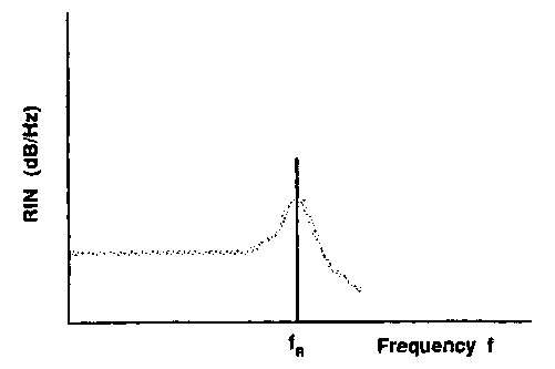
The transmitting laser contributes noise to the system in a fashion that is, generally speaking, proportional to the peak transmitted laser power. This noise is always evaluated as a fraction of the laser power and is therefore termed relative intensity noise (RIN). The RIN contribution from a laser is specified in dB/Hz, to reflect a spectral density which is approximately flat and at a fixed ratio (expressed in dB) to the laser power. Figure 17 shows a typical plot of the relative intensity noise of a source. The specification of RIN as a flat noise source is valid only at frequencies much less than the relaxation oscillation frequency and in situations where reflections are small.
FIGURE 16 Typical point-to-point optical fiber communications link.
FIGURE 17 Typical RIN spectrum for a diode laser. The peak corresponds to the relaxation resonance frequency, fR, of the laser.
The relative intensity noise is affected rather dramatically by the environment of the diode laser. A rather weak reflection back into the laser will both increase the magnitude of the relative intensity noise and modify its spectrum. As the reflection increases, it can produce self-pulsations and chaos in the output of the laser, rendering it useless for communications applications.37 Thus, the laser cannot be thought of as an isolated component in the communications system. Just as RF and microwave systems require impedance matching for good performance, an optical communications system must minimize reflections. This is relatively easily accomplished for a long distance telecommunications link which makes use of low-reflection fusion splices. However, in a short link-network environment which must be modular, a small number of connectors can cause severe problems unless those connectors are designed to minimize reflections. It is now widely accepted that optical fiber connectors must be specified both in terms of insertion loss and reflection. A 1 percent reflection from a fiber connector can have far more serious implications for an optical fiber link than a 1 percent loss which is not reflected back to the laser. Optical isolators are available but only at considerable expense and are not generally considered economically realistic for network environments.
Impact of Fiber Properties on a Communications Link. For moderate power levels, the fiber is a passive, dispersive transmission channel. Dispersion can limit system performance in two ways. It results in a spreading of data pulses by an amount proportional to the spectral width of the source. This pulse spreading produces what is commonly termed "intersymbol interference." This should not be confused with an optical interference effect, but is simply the blurring of pulse energy into the neighboring time slot. In simple terms, it can be thought of as a reduction in the modulation depth of the signal as a function of link length. The effects of dispersion are often quantified in the form of a power penalty. This is simply a measure of the additional power required to overcome the effects of the dispersion, or bring the modulated power to what it would be in an identical link without dispersion. It is commonly expressed as a decibel ratio of the power required at the receiver compared to that of the ideal link.
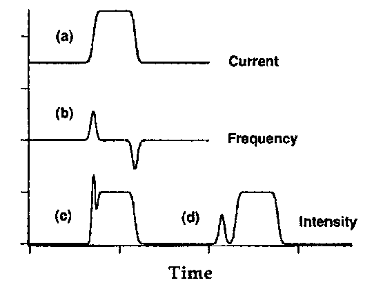
Modulation-induced frequency chirp of the laser source will also result in pulse distortion. This is illustrated in Fig. 18, in which the drive current of the laser is modulated. The accompanying population relaxation produces a frequency modulation of the pulse. Upon transmission through a dispersive link, these portions of the pulse which are "chirped" will be advanced or retarded, resulting in both pulse distortion and intersymbol interference.
FIGURE 18 Modulation of the drive current in a semiconductor laser (a) results in both an intensity (b) and a frequency modulation (c). The pulse is distorted after transmission through the fiber (d).
System Design. The optical receiver must, within the signal bandwidth, establish an adequate signal-to-noise ratio (SNR) for accurate regeneration/retransmission of the signal. It must accomplish this within the constraints of the fiber dispersion and attenuation, the required system bandwidth, and the available source power. First-order system design normally requires the following steps:
1. Determine the maximum system bandwidth (or data rate for digital systems) and the appropriate transmission wavelength required for the system.
2. Find the maximum source RIN allowable for the system. For analog systems, in which a signal-to-noise ratio (SNR) must be specified in a bandwidth Bn, the RIN (which is usually specified in dB/Hz, indicating a measurement in a 1-Hz bandwidth) must obey the following inequality:
The SNR is specified here as an absolute ratio of carrier power to noise power. For an SNR specified as a decibel ratio,
For digital systems, a Gaussian assumption allows a simple relationship between error probability (also termed bit error rate) and the signal-to-noise ratio:
Where erfc denotes the complementary error function and the decision threshold is assumed to be midway between the on and off states. The maximum error probability due to source noise should be considerably less than the eventual target error probability. For system targets of 10-9 to 10-12, the error probability due to source RIN should be considerably less than 10-20. This will allow at least a 3-dB margin to allow for increases in RIN due to device aging.
3. Establish a length limit associated with the source frequency chirp and spectral width. The frequency chirp af is specified in GHz per milliampere change in the drive current of the laser. A total current modulation Im therefore yields a frequency deviation Af of
This frequency deviation translates into a propagation delay via the fiber intramodal dispersion D. This delay must be kept less than the minimum pulse width (data rate). With D specified in ps/nm-km, the length in kilometers must obey the following inequality to avoid penalties due to frequency chirp:
where B denotes the data rate and is the reciprocal of the pulse width for data pulses that fill up an entire time slot. (These signals are designated non-return-to-zero, or NRZ.)
The length limit due to source spectral width Av obeys a similar inequality—in this case, the delay associated with the spectral spread of the source must remain much less than one pulse width:
If the chirp is low and the unmodulated source bandwidth is less than the system bandwidth being considered, one must require that the delay distortion of the signal spectrum itself be small compared to a pulse width, requiring
For multimode fiber systems, the limiting length will generally be associated with the inter-modal dispersion rather than the material and waveguide dispersion. A length-bandwidth product is generally quoted for such fibers. With the length and bandwidth limits established, it is now possible to design, within those limits, a receiver which meets the necessary specifications.
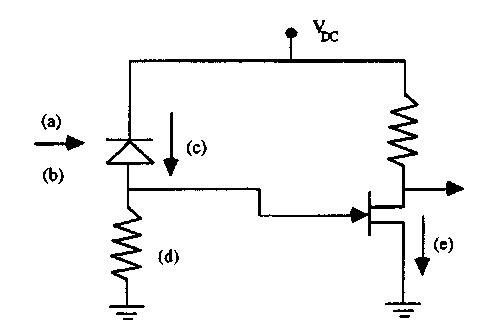
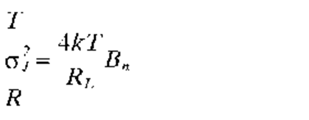
4. Determine the minimum power required at the receiver to achieve the target SNR or error probability. This minimum acceptable power (MAP) is first computed assuming an ideal source (no RIN contribution). A correction for the RIN can be carried out later. A computation of the MAP requires a knowledge of the noise sources and detector bandwidth. It is conventional to express the noise sources in terms of equivalent input noise current sources. The noise sources of importance for such systems are: the shot noise of the photocurrent, dark current, and drain current (in the case of a field effect transistor (FET) preamplifier); the Johnson noise associated with the load resistor or equivalent amplifier input impedance; 1/f noise from certain classes of FETs. The noise contributions from amplifiers other than the first stage are generally second-order corrections. Figure 19 shows a schematic of the receiver and relevant noise sources. Table 3 gives expressions for, and definitions of the important physical quantities which determine the receiver sensitivity.
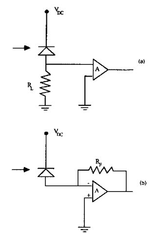
Figure 20 illustrates two possible configurations for the detector/amplifier combination. Of these, the integrating front end is the simplest (particularly for high-frequency operation) but tends to be slower than a transimpedance amplifier with an equivalent load resistance. This is because the transimpedance amplifier reduces the effective input impedance of the circuit by (A + 1), where A denotes the open loop gain of the amplifier.
FIGURE 19 Schematic of the receiver, showing the introduction of noise into the system. Noise sources which may be relevant include (a) signal shot noise; (b) background noise (due to thermal background or channel crosstalk); (c) shot noise from the leakage current; (d) Johnson noise in the load resistor; (e) shot noise and 1/f noise in the drain current of the field effect transistor.
For equivalent bandwidth, the transimpedance amplifier exhibits a lower Johnson noise contribution since a higher feedback resistance is possible. It is worth mentioning that the transimpedance design tends to be much more sensitive to the parasitic capacitance which appears across the feedback resistor—small parasitics across the load resistor tend to be less important for the integrating front end.
The excess noise factor Fe is determined by the choice of detector. There are several choices over the wavelength range generally of interest for optical fiber transmission. (A detailed discussion of the principles of operation can be found in Chaps. 15-17 of Vol. I.)
TABLE 3 Symbols and Expressions for Receiver Noise
FIGURE 20 Two possible configurations for the detector/amplifier: (a) the integrating front end yields the simplest design for high speed operation; (b) the transimpedance amplifier provides an expansion of the receiver bandwidth by a factor of A + 1, where A is the open loop gain of the amplifier.
1. The p-i-n photodiode is described in some detail in Chap. 15 of Vol. I ("Photodetec-tors"). It can provide high quantum efficiencies and speeds in excess of 1 GHz. Dark currents range from less than 1 nA for silicon devices to 1 |iA or more for Ge diodes. The dark current increases and the device slows down as the active area is increased.
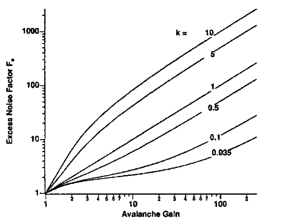
2. The avalanche photodiode is a solid state device which exhibits internal multiplication of the photocurrent in a fashion that is sometimes compared with the gain in photomultiplier tubes. The multiplication does not come without a penalty, however, and that penalty is typically quantified in the form of an excess noise factor which multiplies the shot noise. The excess noise factor is a function both of the gain and the ratio of impact ionization rates between electrons and holes.
Figure 21 shows the excess noise factor for values of k ranging from 50 (large hole multiplication) to 0.03 (large electron multiplication). The former is claimed to be typical of certain III-V compounds while the latter is typical of silicon devices. Germanium, which would otherwise be the clear detector of choice for long wavelengths, has the unfortunate property of having k near unity. This results in maximum excess noise, and Ge avalanche photodiodes must typically be operated at low voltages and relatively small gains. The choice of a p-i-n detector, which exhibits no internal gain, yields Fe = 1.
3. The need for very high speed detectors combined with the fabrication challenges present in III-V detector technology has led to a renewed interest in Schottky barrier detectors for optical communications. A detector of considerable importance today is the metal-semiconductor-metal detector, which can operate at extremely high speed in an inter- digitated electrode geometry.
FIGURE 21 Excess noise factor for an avalanche photodiode with the electron/hole multiplication ratio k as a parameter. Small values of k indicate purely electron multiplication while large values of k indicate purely hole multiplication.
With all noise sources taken into account (see Table 3 for the relevant expressions), the signal-to-noise ratio of an optical receiver can be expressed as follows:
where ![]() denotes the total signal-independent receiver noise:
denotes the total signal-independent receiver noise:
and C is the signal shot noise as in Table 3. If the effects of RIN are to be included, the following correction to the SNR may be made:
With the signal-to-noise ratio determined, the error probability may be expressed in terms of the signal-to-noise ratio
The just-noted expressions assume Gaussian distributed noise sources. This is a good assumption for nearly all cases of interest. The one situation in which the Gaussian assumption underestimates the effects of noise is for avalanche photodiodes with large excess noise. It was shown by McIntyre38,39 and Personick40 that the avalanche multiplication statistics are skewed and that the Gaussian assumption yields overly optimistic results.
5. Given the MAP of the receiver, the fiber attenuation and splice loss budget, and the available pigtailed laser power (the maximum power coupled into the first length of fiber by the laser), it is possible to calculate a link loss budget. The budget must include a substantial power margin to allow for device aging, imperfect splices, and a small measure of stupidity. The result will be a link length which, if shorter than the dispersion limit, will provide an adequate signal-to-noise ratio.
For further link modeling, a variety of approaches can be used to numerically simulate the link performance and fully include the effects of fiber dispersion, a realistic detector-preamplifier combination, and a variety of other factors which the first-order design does not include. Nevertheless, a first-order design is necessary to reduce the range of free parameters used in the simulation.
The ultimate goal of the point-to-point link is to transparently transmit the data (or the analog signal) in such a way that standard communications techniques may be used in the optical link. Examples include the use of block or error-correcting codes in digital systems, standard protocols for point-to-point links between nodes of a network, or frequency allocation in the case of a multichannel analog link.
![tmp8-78_thumb[2][2]_thumb tmp8-78_thumb[2][2]_thumb](http://what-when-how.com/wp-content/uploads/2011/09/tmp878_thumb22_thumb_thumb.png)

![tmp8-86_thumb[2][2]_thumb tmp8-86_thumb[2][2]_thumb](http://what-when-how.com/wp-content/uploads/2011/09/tmp886_thumb22_thumb_thumb.png)
![tmp8-87_thumb[2][2]_thumb tmp8-87_thumb[2][2]_thumb](http://what-when-how.com/wp-content/uploads/2011/09/tmp887_thumb22_thumb_thumb.png)
![tmp8-88_thumb[2][2]_thumb tmp8-88_thumb[2][2]_thumb](http://what-when-how.com/wp-content/uploads/2011/09/tmp888_thumb22_thumb_thumb.png)




![tmp8-103_thumb[2][2][2] tmp8-103_thumb[2][2][2]](http://what-when-how.com/wp-content/uploads/2011/09/tmp8103_thumb222_thumb.png)
