Following optics, the next primary element in any sensor system is the detector. There are two primary detection techniques: film and electronic. We’ll discuss film systems briefly, and then modern solid-state electronic systems.
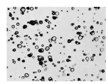
Figure 3.24(a) The silver bromide grains of an x-ray film emulsion (2,500 diameters).
Figure 3.24 (b) Cross section of the unprocessed emulsion on one side of an x-ray film.
Note the large number of grains as compared to the developed grains in the figure at right.
Figure 3.24 (c) Cross section showing the distribution of developed grains in an x-ray film emulsion exposed to give moderate density.
Film
Film is made up of two elements, a flexible, transparent base, and a light-sensitive emulsion, generally a gelatin containing a radiation-sensitive silver compound. These silver salts undergo subtle atomic changes when exposed to light. Treating the exposed film with a chemical solution called a developer causes a reaction to take place that results in the formation of black, metallic silver. It is this silver, suspended in a gelatin, that constitutes the image. Figure 3.24, taken from a Kodak illustration, shows how the grains appear and the range of grain sizes [Fig. 3.24(a)], and then how the grains change with exposure and development.
The resolution of film depends on the size of these silver grains—higher resolution requires finer grain. The tradeoff is that faster, or more sensitive, films require larger silver-halide grains (think larger cross-section, and higher chance of a photon hitting the crystal). For the Corona missions, Kodak developed special films that had very high resolution (100-160 lines/mm), but were correspondingly slow. The large optics helped compensate for the low sensitivity.
Solid state
Generally speaking, the detectors involved in remote sensing utilize arrays of solid-state detectors, much like the charge-coupled devices (CCDs) in modern video cameras and digital still cameras. This rather broad statement about the class of sensors also termed focal plane arrays (FPAs) does not properly account for the many sensors flying linear arrays (1D focal planes), as on SPOT, or even the ongoing use of single-detector sensors such as on GOES and Landsat. Still, the underlying physics is similar.
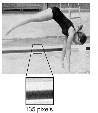
Figure 3.25 This photograph was taken on Kodak Tri-x pan film—an old standby for action photography, which was characteristically grainy. The small box on the gutter defines the expanded region. The image was scanned at 4000 lines per inch, so the 135 pixels correspond to 0.857 mm (0.03375 in.).
There are a number of possible approaches to electronic detection of optical radiation. The focus here is on "intrinsic" (bandgap) detectors, which is the design used for most silicon (CCD) focal planes.
As with Bohr atoms, solid materials (in particular, semiconductors) have a distribution of energy levels that may be occupied by electrons. Generally, electrons reside in a state corresponding to the ground state of an individual atom, termed the valence band. There is then a gap in energy (a "bandgap") that represents a range of energies that are forbidden for the electron to occupy.
Figure 3.26 Energy band gap illustration.
If a photon hits the semiconductor, however, it can give energy to an electron in the valence band, exciting it up into the conduction band. The significance is that it is now possible for the electron to move as if in a conductor, and it can be collected and measured. This is the essence of the detection mechanism for most solid-state detectors. Their efficiency varies, but typically 40-80% of incident photons with sufficient energy can be detected. For silicon, the maximum efficiency occurs in the near infrared, from 0.9-1.0 ^m.
This simple description makes it possible to understand some of the more important constraints in the use of solid-state detectors. First, one must match the energy bandgap to the energy of the photons to be observed. The photon energy must be greater than the size of the bandgap, which varies with material.17’18
Table 3.1 Bandgap energies for common semiconductors.
How do these values limit the use of different materials as detectors? Taking silicon as the most common example:
Here,![]() is the bandgap energy
is the bandgap energy![]() and we use:
and we use:
So, the visible and the first part of the near-infrared spectrum can be detected with silicon detectors. This is reflected in their common use in modern cameras.
The detection of longer wavelength photons requires materials such as HgCdTe, or InSb. The relatively small band gaps cause a problem, however. At room temperature, the electrons tend to rattle around, and every now and then one will cross the gap, due to thermal excitation. This process is largely controlled by the exponential term that comes from the "Maxwell-Boltzmann" distribution (or bell-shaped curve), which describes the velocities, or energies, to be found in any collection of objects (whether electrons, atoms, or molecules) in a thermal equilibrium:
If these electrons are collected, this becomes part of a background noise known as the dark current. To prevent this, the materials must be cooled—typically to 50-70 K, which requires liquid nitrogen at least, and for some applications, liquid helium (4 K).
Figure 3.27 Rough guide to the spectral ranges of use for different focal-plane materials. HgCdTe is abbreviated as MCT: MerCadTelluride.
Mechanical refrigerators can also be used, but are problematic in space applications because they generally have relatively short lifetimes, and can introduce vibration into the focal plane, which is bad. Some recent NASA missions have used a long-lived pulse-tube technology developed by TRW, with apparent success.
The importance of cooling is illustrated here with a calculation:
Use HgCdTe, assume a bandgap of 0.1 eV, and compare the nominal number of electrons above the bandgap at room temperature (300 K) and at 4 K. Note that the conversion factor k in the term kTis:
At room temperature, the exponential is small, but reflects a non-negligible number of excitations of electrons above the bandgap energy. At the temperature of liquid helium, the electrons sit quietly below the band gap. Figure 3.27 shows the wavelength and temperature ranges that may be used for a variety of materials. Note how longer wavelengths fairly uniformly require lower temperatures.
Visible imaging cameras uniformly use silicon as the sensitive element. Typical commercial infrared imaging systems use InSb, PtSi, and HgCdTe (e.g., the FLIR Systems family of cameras). In addition, there are two popular new technologies: quantum-well (QWIP) and microbolometer detectors. The latter in particular offers a variety of advantages over the more traditional cooled semiconductor systems, as discussed below.
Focal plane arrays
The photosensitive component of a detector can exist as a single element, and there are a number of operational systems that nominally have a single detector. A notable current example would be the GOES weather satellite, described later. Generally, however, newer systems feature either rectangular arrays (as in digital cameras) or linear arrays of pixels, as will be seen below for IKONOS, with an array of 1 x 13,500 pixels.
A CCD is an array of sensitive elements. The CCD is an integrated circuit (IC) with the unique property that a charge held in one cell of the IC can be shifted to an adjacent cell by applying a suitable shift pulse. Information defined by the amount of charge can be shifted from cell to cell with virtually no loss. This characteristic allowed the devices to be used as a memory device. When it was further discovered that the construction could be altered so that individual cells also responded to incident light while retaining the ability to shift charges, the concept of a solid-state imager emerged.
In a CCD, each picture element, or pixel, converts incoming light into an amount of charge directly proportional to the amount of light received. This charge is then clocked (shifted) from cell to cell, to be finally converted to a video signal that represents the original image, at the output of the CCD.
The detector resolution is defined by the pitch, or spacing, between individual pixel elements on the focal plane, which is typically very close to the size of the pixel. Modern silicon sensors generally have a pitch on the order of 5-10 |m. More exotic materials generally have somewhat larger values for the detector pitch.
Uncooled focal planes: microbolometers
One problem with the technology behind semiconductor detectors is the need for cooling. Either a coolant (e.g., liquid nitrogen) or a mechanical refrigerator is required. The former is awkward in the field and limited for space use, because only so much coolant can be brought along. Mechanical devices are generally troublesome and tend to fail in space applications. Consequently, there is significant motivation to develop alternatives. Energy detectors, as opposed to the photon detectors described above, are emerging as an important alternative for remote sensing systems.
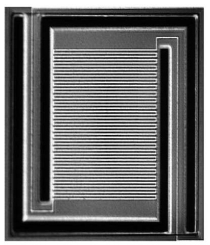
Figure 3.28 Thermally isolated resistor (200 |m x 200 |m), used in a microscopic Wheatstone bridge. Current enters from top left and exits through the bottom right. As the sensor heats, changes in its resistance can be measured with great sensitivity.
Microbolometer techniques approach detection by sensing the change in temperature of a sensitive element, typically by measuring its resistance. This allows the direct detection of "heat," as opposed to counting photons directly. Consequently, such detectors do not need to be cooled. Commercial IR cameras are now using these detectors, and they are very popular for applications such as firefighting. These cameras are not as sensitive as photosensitive technologies and may not offer the spatial resolution of traditional approaches, because the pixel pitch is generally fairly large, on the order of 50 ^m with current detectors.


