ABSTRACT
Ultrafine-grained (UFG) metals possess grain sizes on the order of hundreds of nanometers and display a remarkable capacity for high strength, high ductility, and enhanced superplasticity. This paper presents the preparatory steps necessary for a high-resolution experimental investigation into the deformation mechanisms active in UFG metals. A new experimental methodology is used, in which an optical metrology known as Digital Image Correlation (DIC) is combined with scanning electron microscopy to track the quantitative development of full-field strains on the length scale of the microstructure. The micro-scale field of view and use of a SEM for image capture require the development of novel specimen patterning methods and of image distortion corrections prior to experimentation. The results obtained through the combined SEM and DIC approach, and corresponding pre- and post-mortem electron backscatter diffraction (EBSD) analysis, enable the analysis of the real-time, micro-scale evolution of Lagrangian strains at an unprecedented spatial resolution, and the quantification of the surface deformations inside grains and across grain boundaries as the material is subjected to thermo-mechanical loading.
TECHNICAL APPROACH
To track the in-situ development of strain, the optical method Digital Image Correlation (DIC) is used to measure displacements on the surface of the test sample from which Lagrangian strains can be calculated. DIC requires the sample surface to have isotropic, high contrast random variations in surface features, taken generally as brightness or roughness. The surface is broken up into subsets, and the displacements and thus Lagrangian strains are then calculated by tracking the change in surface features at each subset as the sample is deformed, as shown in figure 1. For macroscopic testing, patterning is most commonly achieved by applying a random speckle pattern with an airbrush. This work will utilize a SEM for small-scale imaging of the tensile sample as it is heated and strained in a tensile/compression stage. As a result of the small size scale investigated in this work, it was necessary to develop new patterning techniques, which are detailed in the sample preparation section of this paper.
Tensile samples fabricated by wire Electro-Discharge Machining (EDM) from extruded super-purity (99.99%) aluminum and 6061-T6 aluminum sheets were used for development of the techniques necessary for this combined SEM-DIC investigation. The 99.99% Al and 6061-T6 Al tensile samples have 2.5 x 4 mm and 1 x 4 mm gage cross sections respectively, and 6 mm gage lengths.
Fig. 1 Illustration of a DIC subset tracking surface brightness as a test sample is deformed
SAMPLE PREPARATION
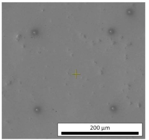
The first step following fabrication of the tensile samples is preparing the surface for microstructural analysis through Electron Backscatter Diffraction (EBSD). This is achieved by polishing with 400, 600, and 800 grit SiC papers with water. Buehler MetaDi Supreme polycrystalline 9, 3 and 1 pm diamond suspensions are then used followed by Buehler MasterMet colloidal silica suspension. After polishing, the test Field of View (FOV) is marked with a FEI Quanta 200 3D SEM equipped with a Focused Ion Beam (FIB) and Gas Injection System (GIS). Through the use of the GIS, platinum markers are deposited on the surface of the test sample at the corners of the desired FOV as shown in figure 2. One additional marker is placed outside of the field of view to assist in the determination of the test sample orientation.
The dark rings surrounding the markers in figure 2 are a result of the ion beam current being set too high and can be removed by reducing the current accordingly. The platinum markers adhere very well to the surface of aluminum test samples and are capable of withstanding light polishing with colloidal silica as well as ultrasonic cleaning. Following the application of the platinum markers to the test sample, a pretest EBSD map of the sample surface is collected. The markers assist in aligning both the pre- and post-test EBSD area with the test image FOV.
There have been a limited number of papers on the application of a small-scale pattern suitable for DIC in a SEM [1-3]. Therefore a full survey of patterning methods has been performed to determine the most suitable methodology. The first method investigated was a chemical vapor thin film rearrangement method [1]. After multiple attempts and variations in film thickness, vapor temperature, and sample surface roughness, repeatable results could not be achieved by the investigators. Small areas of the film appeared to break up as desired, but the islands were dispersed and the majority of the film remained intact. Previous work by Sabate et al. [4] used a FIB to mill a random pattern into the surface of a test sample. The method described is semi-destructive and cannot be used in current tests as the surface of the sample is actually milled away in areas.
Fig. 2 Platinum markers applied to the surface of a 6061-T6 aluminum test sample to mark the area of interest
However, through the use of a GIS equipped FIB, platinum markers were instead deposited onto the surface of the test sample in order to create a random tracking pattern. The pattern shown in figure 3 was created by drawing a random block pattern in the FIB user interface and depositing it in patches that were translated and rotated to cover the surface. Due to the damage that results from the ion beam, the limitation on the minimum speckle size, and time demand required by this method, it is no longer being used. Evaporating metal through TEM grids has been successfully used by Biery et al. [5] in the past to apply a regular grid to the surface of a test sample. In an attempt to generate a random pattern using a similar method, alumina and polycarbonate filter membranes acted as templates for the evaporation of gold onto test sample surfaces. While this method was successfully applied to TEM grids consisting of 7.5 x 7.5 ^m holes, the aspect ratio (Thickness:Pore Diameter, alumina: 325:1, polycarbonate: 25:1) of the pores in the alumina and polycarbonate membranes proved too large and this technique did not yield a suitable pattern.
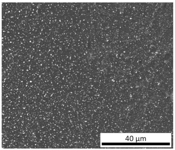
Patterning is currently being performed successfully with gold nanoparticles (NPs). Gold NPs can be purchased in sizes ranging from 2-200 nm and have high contrast when imaged with a SEM, making them good candidates for patterning for DIC-SEM experimentation. In the current work, concentrated solutions of gold NPs supplied by Ted Pella are used to create DIC tracking patterns. Numerous methods have been investigated to determine the effect of drying temperature, angle, airflow, and atmospheric pressure on the NP distribution. Additionally, layering methods have been investigated, such as applying a second NP layer to a previously dried layer, and alternating NP layers with sputtered carbon layers. NP patterning has been successful in providing a suitable tracking pattern for DIC-SEM and is a quick process, requiring only the time for the solution to dry, results in a broad distribution of speckle sizes, and provides a high contrast pattern when imaged with the secondary or backscatter electron detector as shown in figure 4.
Fig. 3 FIB pattern created by translation and rotation of a small user generated pattern. The white spots are platinum and the substrate is pure aluminum
To pattern with NPs, droplets of the NP solution are applied with a micro-pipette or plastic dropper. Prior to application, the NP solution is held in an ultrasonic cleaner for 15 minutes to break up aggregates and distribute the NPs throughout the solution. It has been determined that drying time is a critical parameter in the quality of the speckle pattern generated by NPs. A long drying time encourages the NPs to clump and results in an inhomogeneous dispersion with the majority of the
Fig. 4 DIC appropriate 100 pm field of view SEM image of a 100 nm diameter gold nanoparticle pattern on a polished Aluminum sample
NPs formed as large aggregates at the outer edge. Additionally, the drying behavior of the NP solution varies greatly depending on the surface energy of the substrate to which it is applied. For example, the droplet has a very small contact angle with freshly polished pure aluminum. However, over time the oxide layer adsorbs polar water molecules from the atmosphere, which results in a decreased surface energy [6,7]. As a result, the contact angle between the aluminum substrate and the NP droplet increases. This large contact angle increases the drying time and results in more aggregates. Different drying methods have seen more success on copper and ceramics, therefore it is difficult to predict the drying behavior on different substrates.
To accurately calculate surface displacements, the NPs must remain securely attached as the sample is strained. It has been determined that the NPs strongly adhere to the surface of Al test samples, ensuring fidelity of the deformation tracking. Tests were performed in which the FIB was used to mill markers on the surface of 99.99% Al and 6061-T6 Al test samples. NPs were deposited in the marked area and the sample was strained in a tensile stage inside the SEM chamber. Average strain values calculated from the NPs by the DIC program matched the values calculated from measuring the motion of the FIB milled markers used as an "extensometer". Additionally, in later tests, there was no noticeable change in NP density after rinsing the sample surface with a strong jet of water from a squirt bottle. NPs were also not observed outside of the original droplet area, further verifying that the rinse did not remove particles from the surface. To remove the NPs from the surface for post-test EBSD, the sample is held in de-ionized water in an ultrasonic cleaner for ten minutes. Even after this cleaning, NPs still remain on the surface but their distribution is so diffuse that they interfere only minimally with the EBSD mapping. Shortcomings of NP patterning include difficulty in preventing aggregates and the difficulty in achieving consistent results on different substrates. However once the drying behavior on the desired substrate is determined, it is a fast and cost effective patterning method. Electron beam lithography is currently being investigated as a patterning methodology for comparison with NP patterning.
SEM DISTORTION CORRECTION
Two forms of distortion exist in images captured by a SEM; drift or temporal distortion and spatial distortion. If not corrected, these distortions will unacceptably affect displacement and strain calculations. Drift distortion arises from errors in the positioning of the electron beam as it raster scans across the field of view. It varies with time and appears as displacements between pixels that vary throughout the image scan. Spatial distortion results from the complex focusing mechanism used in the SEM and appears as curvature of the displacement field that is nearly constant throughout all images.
In this work, it was observed that changes in chamber pressure and scan speed as well as sample charging all have a significant effect on drift distortion. Low chamber pressure at the beginning of the imaging process for a 100 pm Horizontal
Field Width (HFW) led to apparent displacements of 4 pixels in a single image. In images of non-conducting alumina filters that had been sputter coated with gold, apparent displacements of up to 25 pixels in a single image were observed. For a 100 pm HFW, 25 pixels corresponds to over 2 pm of drift. Charging artifacts were not seen in the images, but are most likely responsible for the large apparent drifts. Drift distortion accumulates over the period of the test leading to inaccurate results.
To correct for distortion, the procedure as outlined in references [8,9] was followed and subsequently built upon.
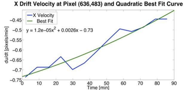
Fig. 5 Drift velocity at one pixel location over the calibration phase and the best-fit quadratic curve
In summary, 20-30 images of a speckle patterned surface are captured using a FEI Quanta 3D 200 SEM with the time as well as the pressure at which each image is captured being recorded. The images are captured in pairs where the specimen remains stationary in the pair. Between image pairs, the specimen is translated a known distance in the horizontal and vertical directions. Translations are performed manually with the stage control knobs since translations by inputting the desired value in the SEM user interface prove too aggressive and result in additional unknown displacements being incorporated in the images. DIC is performed on each image pair through the use of VIC2D software developed by Correlated Solutions Inc. The raw displacement data exported by VIC2D is then imported into a custom Matlab code created by the investigators for distortion correction.
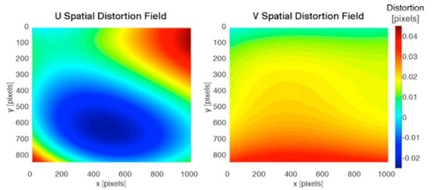
Fig. 6 Spatial distortion fields for a 300 ^m horizontal field width
The Matlab code first determines the time that passed between each DIC data point being scanned in the first and second image of every image pair. The u and v drift velocity at the midtime of each stationary image pair at every data point is calculated and plotted against time allowing for visualization of the change in drift velocity over the time of the calibration phase. A quadratic function is then fit to the velocity data for each data point and integrated over time so that the drift distortion can be determined over any time frame. Using each data point’s unique drift function, all of the calibration image data is corrected for drift distortion before being used for spatial distortion correction. A plot of the u drift velocity at one data point and the quadratic best-fit curve is shown in figure 5. By capturing calibration image pairs throughout the test phase, the drift distortion function for each pixel can be modified as needed to account for any changes in drift. The relationship between the chamber pressure and drift is currently being investigated as a means to better characterize the evolution of drift.
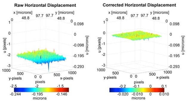
Spatial distortion does not vary between test images, but it can change between tests due to the replacement of the SEM filament or aperture alignment. It is corrected by correlating the images captured before and after each translation. Since the sample has only experienced rigid body motion, the displacement fields should be flat and any deviation from the correct, flat displacement field is determined at each data point and subtracted from the displacement data in all calibration and test images. A typical u and v spatial distortion field for a 300 ^m HFW is shown in figure 6. Pixel displacement values for a stationary image pair before and after distortion correction can be seen in figure 7. Note that the displacement average is shifted to zero and the magnitude of the variation in displacement is reduced by an order of magnitude. After correcting all of the VIC2D displacement data for distortion the Matlab code calculates the Lagrangian strain at each data point.
Fig. 7 Raw horizontal (u) displacement and distortion corrected u displacement for a stationary image pair. The distortion correction code shifts the displacement average closer to zero and reduces the magnitude of the variation in displacement by an order of magnitude
TEST ON COARSE-GRAINED 6061-T6 ALUMINUM
In order to validate the developed procedures, tests have been performed on coarse-grained 6061-T6 Al. A tensile samples with a gage cross section of 0.6 x 4 mm and gage length of 6 mm was polished as outlined in the sample preparation section. Immediately after polishing, platinum parkers were applied with a FIB and a pre-test EBSD map of the surface as shown in figure 8a was collected using a step size of 2 ^m. After EBSD, 200 nm diameter gold NPs were deposited on the sample with a micropipette.
Following drying of the NP solution, the sample was loaded into a Kammrath & Weiss tensile/compression stage in the FEI Quanta 200 3D SEM. Calibration images were captured, and the sample was strained to an elongation of 13.75%, resulting in visible deformation in the area of interest. The sample was strained in steps of on average 20 ^m or 6.7°% of the HFW, which allowed for good correlation in VIC2D. After each step, the sample was held for approximately 30 seconds to allow the load to stabilize. Every 5 to 10 images, image pairs were captured to compare to the drift distortion quadratic fit. Upon reaching the maximum elongation, the load was removed and a final image was captured of the unloaded sample. Following the tensile test, the NPs were removed and a post-test EBSD map was collected as shown in figure 8b.
Fig. 8 a) Pre-test EBSD map of 6061-T6 Al sample. b) Post-test EBSD map corresponding to the unloaded sample FOV that was captured in the final test image. c) !xx overlaid EBSD map showing areas of high strain primarily at grain boundaries. The black rectangles are covering up the locations of the platinum markers.
Figure 8c shows the post-test EBSD map overlaid with the distortion-corrected strain (!xx) along the loading axis (x), showing the highest strains occurring primarily at the grain boundaries. Through the use of DIC, the evolution of strain can be observed throughout the test. This allows the investigators to pinpoint location of strain concentrations as they develop and observe the strain evolve throughout the loading. Work is currently underway to develop a method to determine the relative displacements at areas of high strain. This will allow the determination of active deformation mechanisms, and the characterization of the development and interaction of these mechanisms as the sample is thermomechanically loaded.
CONCLUSIONS
Significant work has been performed to develop the novel experimental methodologies required for successful DIC-SEM analysis of deformations on the scale of the microstructure. From work performed thus far, the following conclusions have been made:
1. Gold nanoparticles can effectively be used to create a DIC pattern for SEM imaging. Patterning methods for deformation tracking will continue to be investigated, including improvements on nanoparticle patterning and the use of electron beam lithography as a secondary patterning methodology.
2. The developed distortion correction codes successfully remove both drift and spatial distortions from SEM micrographs. The fit equations generated during calibration correctly predict the distortion throughout the test period. The code also accurately calculates the Lagrangian surface strains from these distortion corrected displacements.
3. Through the use of platinum markers to mark the area of interest, OIM maps of the sample surface can be accurately matched up with test images and the DIC calculated strain field. This methodology will enable the quantification of deformation mechanisms active in UFG metals.
It has also been displayed that distortion correction is critical to obtain accurate results from DIC experiments performed in an SEM. Future experiments will be performed on UFG 99.99% pure aluminum through the use of the outlined methodologies.

