4.3
The three-phase voltage source inverter (VSI) is shown in Figure 4.13. The voltage source for the inverter is made up from a rectifier and the so-called dc link, composed of a capacitor, C, and inductor, L. If the ac machine fed from the inverter operates as a motor (i.e., in the first or third quadrant), the average input current is positive. However, the instantaneous input current, iv may assume negative values, absorbed by the dc-link capacitor which, therefore, is necessary. The capacitor also serves as a source of the high-frequency ac component of iv so that it is not drawn from the power system via the rectifier. In addition, the dc link capacitor smooths and stabilizes the voltage produced by the rectifier. The optional dc-link inductor is less important, being introduced to provide an extra screen for the power system from the high-frequency current drawn by the inverter.
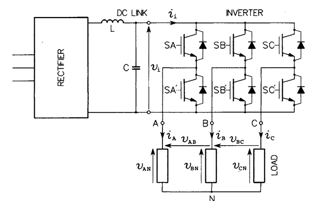
FIGURE 4.13 Voltage source inverter.
Clearly, the topology of the voltage source inverter represents an inverse of that of the current source PWM rectifier in Figure 4.12 (note that the load of the inverter contributes the inductances corresponding to input inductances, L{, of the rectifier). Here, the freewheeling diodes provide alternative paths for output currents. Both semiconductor power switches in a given leg (phase) of the inverter may not be on simultaneously, because they would short the input terminals. On the other hand, with both switches off, the output voltage would be indeterminable, because the potential of the respective output terminal would depend on which diode is conducting the output current in that phase. This would make the open-loop control of the output voltage impossible. Therefore, voltage source inverters are so controlled that one switch in each leg is on and the other is off. In this way, the turned-on switch connects one of the input terminals to the output terminal, and potentials of all three output terminals are always known. To avoid the so-called shot-through, that is, potentially damaging simultaneous conduction of both switches in the same leg, turn-on of a switch is delayed a little with respect to turn-off of the other switch. This delay, on the order of few microseconds, is called a dead time or blanking time.
The voltage source inverter can operate in both the PWM mode and the so-called square-wave mode, characterized by rectangular waveforms of the output voltage. The square-wave operation yields the highest voltage gain of the inverter, but the quality of output current is poorer than that in the PWM mode.
Figure 4.14 shows the current source inverter (CSI) which, in the square-wave mode, produces rectangular waveforms of the output current. For consistency, IGBTs are shown here as the inverter switches, but practical current source inverters are often of such a high power that they must be based on GTOs or SCRs with commutating circuits (to turn the SCRs off). The current-source supply is provided by a controlled rectifier with closed-loop current control and the inductive dc link. The inverter differs from its voltage source counterpart by the absence of freewheeling diodes, which are unnecessary because the constant input current is never negative.
Addition of capacitors at the output allows for PWM operation of the current source inverter. These capacitors are marked in Figure 4.14 using broken lines. The switching action of inverter switches results in pulsed waveforms of currents ia, ib, and ic, but the capacitors shunt most of the high-frequency harmonic content of these currents. Thus, waveforms of the output currents, iA, iB, and ic, are rippled sinusoids. This inverter is an inverse of the voltage-source rectifier in Figure 4.8.
Recently, multilevel voltage source inverters have been receiving serious attention. They allow for higher voltage ratings than the classic inverter in Fig. 4.12 and produce currents of higher quality, albeit at the expense of a higher device count. The number of levels is meant as the number of values of the voltage at an output terminal of the inverter. For instance, in the voltage source inverter described before, each terminal can be
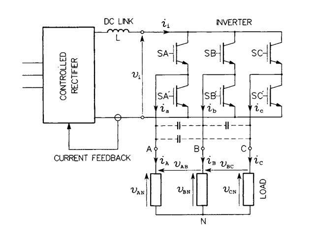
FIGURE 4.14 Current source inverter.
connected to either the positive or negative dc bus and the inverter can therefore be termed as a two-level inverter. The most common, so-called neutral-clamped, three-level inverter is shown in Figure 4.15. Each leg of the inverter is composed of four semiconductor power switches, Sj through S4, with freewheeling diodes, Dt through D4, and two clamping diodes, D5 and D6, that prevent the dc-link capacitors from shorting. The dc link is based on two input capacitors, Q, forming a capacitive voltage divider and an input inductor, L4 (optional).
Although the presence of 12 semiconductor power switches in the three-level inverter implies a very high number of possible inverter states, only 27 states are employed in practice. Specifically, each leg of the inverter is allowed to assume one of the three following states: (1) SI and S2 are on, S3 and S4 are off; (2) S2 and S3 are on, SI and S4 are off; and (3) SI and S2 are off, S3 and S4 are on. It can be seen that the dc input voltage, V{, is always applied to a pair of series-connected switches. Therefore, the voltage rating of a three-level inverter can be twice as high as the rated voltage of the switches.
All the inverters described are characterized by hard switching, that is, each semiconductor switch turns off while carrying a nonzero current and turns on under a nonzero voltage. As a result, each switching is associated with certain energy loss. High switching frequencies, necessary for high quality of the output current, reduce efficiency of the inverter. Side
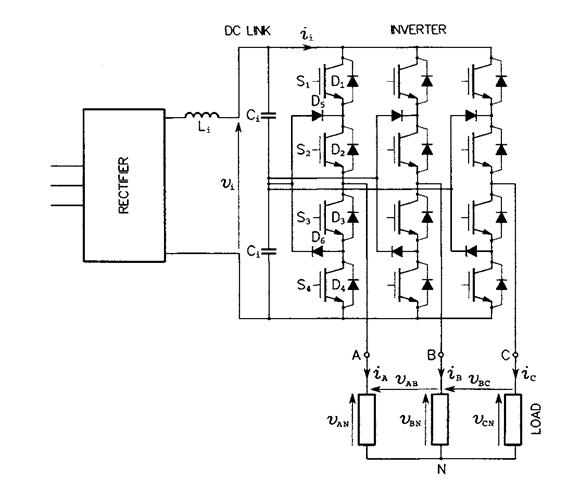
FIGURE 4.15 Three-level neutral-clamped inverter.
effects of hard switching, such as the radiated electromagnetic interference (EMI) or overvoltages in long cables connecting the inverter to the load, are also a problem. Therefore, a great amount of research and development effort has been devoted to soft-switching inverters. Generally, two types of soft switching can be distinguished, zero-voltage switching (ZVS) and zero-current switching (ZCS). Many topologies of soft-switching inverters have been developed within the last decade.
The classic resonant dc link (RDCL) inverter shown in Figure 4.16 employs the ZVS principle.
The supply rectifier with the dc link capacitor C1 and inductor Lx (optional) constitute the dc voltage source for the inverter. Inductor L2 and capacitor C2 form a resonant circuit, the resonance in which is triggered by simultaneous turn-on of both switches in a leg of the inverter, followed by turn-off. When voltage across capacitor C2 reaches zero, ZVS conditions are created for inverter switches. The active clamp based on the capacitor C3 and switch S is used to clip the resonant pulses of the output voltage. Without the clamp, the voltage pulses, whose amplitude largely exceeds the dc supply voltage, would impose unreasonably high voltage rating requirements on the switches and diodes of the inverter.
One phase (phase A) of the auxiliary resonant commutated pole (ARCP) inverter is shown in Figure 4.17. Capacitors Q and C2 form the dc link. To minimize high dynamic stresses on main switches, SA and SA’, a resonant snubber, based on the inductor LA and capacitors CA1 and CA2, is employed. The resonance is triggered by turning on the
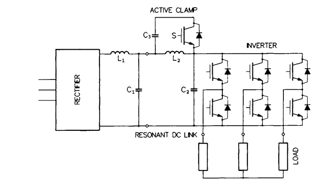
FIGURE 4.16 Resonant dc link inverter.
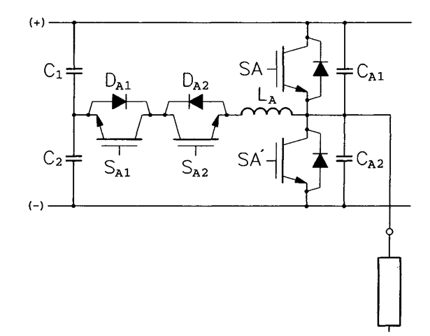
FIGURE 4.1 7 One phase of the auxiliary resonant commutated pole inverter.
bidirectional switch, composed of auxiliary switches SA1 and SA2 and their antiparallel diodes DA1 and DA2. This allows for ZVS conditions for the main switches. The auxiliary switches are turned on and off under ZCS conditions.
ARCP inverters, typically designed for high power ratings (in excess of 1 MVA), provide highly efficient power conversion. In contrast to the RDCL inverter, whose output voltage waveforms consist of packets of resonant pulses, the ARCP inverter is capable of true pulse width modulation. Typically, IGBTs (insulated-gate bipolar transistors) or GTOs (gate turn-off thyristors) are used as the main switches, while MCTs (MOSFET-controlled thyristors) or IGBTs serve as the auxiliary switches.
