Layout Considerations and Simulation Results
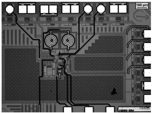
Figure 3-9 shows a microphotograph of the designed dual-gain LNA. The emitter-degenerating inductances, the power supply decoupling capacitors, and the amplifier connection pads can be clearly identified.
The VDD decoupling capacitors filter out any bias noise and help improve LNA stability, which is of concern due to capacitive and bondwire coupling between the bias voltage and RF input/output pins. RF pads rely solely on the top thick layer of metal to minimise parasitic capacitance. The size of the LNA’s chip (including decoupling capacitors and pads) is 1×1.5mm2.
VDD and GND pads are double, allowing two bondwires to reduce their parasitic inductance. Therefore, AC ground and supply loops resulting from bondwire and package parasitic inductances are less significant, reducing the risk of undesired oscillations.
To analyse realistic situations through simulation, different parasitic effects must be taken into account. To obtain realistic results, the simulation setup includes the effects of PAD parasitic capacitances, bondwire inductances, bondwire coupling between different pins, and package parasitics, among others.
The block requirements reported in the previous topic and post-layout simulation results of the LNA are shown in Table 3-3.
Due to the strict specifications previously set, the performance of the receiver will not be seriously affected by the fact that the gain and noise figure of the LNA are slightly worse than specified. Moreover, the gain of other front-end blocks will be increased to compensate for the lower gain in this stage. In addition, as the noise figure is slightly higher, a marginally worse performance of the receiver will be expected in regards to the C/N0.
Figure 3-9 LNA microphotograph
TABLE 3-3 Post-layout results
|
Parameter |
Specifications |
Post-layout |
Unit |
||
|
Gmin |
Gmax |
Gmin |
Gmax |
||
|
S11 |
-18.2 |
-14 |
dB |
||
|
S22 |
-7.6 |
-21.8 |
dB |
||
|
Gain |
20 |
8 |
19.7 |
9 |
dB |
|
NF |
2.5 |
10 |
2.8 |
10.8 |
dB |
|
Current |
7.5 |
mA |
|||
RF Pre-Amplifier and Mixer
To obtain the required gain and noise figure in the down-conversion stage, an RF preamplifier has been implemented before the mixer. The following subsections describe and present the design and combined performance of both blocks (pre-amplifier and mixer).
RF Pre-Amplifier
The input signal of the RF amplifier comes from an external SAW filter, so the input impedance must be 50Q to maximise transferred power and not degrade SAW filter performance due to mismatched impedance.
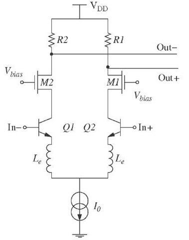
Even though the RF amplifier input signal is single-ended, a differential structure has been selected based on its advantages (see Table 3-4).
The inductive degeneration common emitter differential amplifier shown in Figure 3-10 has been chosen to maximise the gain and minimise the noise figure and power consumption.
Mixer
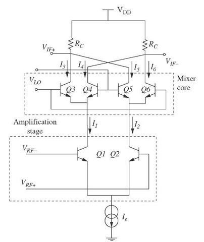
An active mixer has been selected because it presents a higher gain and lower noise than the passive ones. Gilbert mixers are the most widely used active mixers. This mixer is formed by two different stages[Gilbert68]: the amplification stage and the mixing core (see Figure 3-11). In the figure,![]() is the local oscillator voltage input signal,
is the local oscillator voltage input signal,![]() is the radio frequency voltage input signal,
is the radio frequency voltage input signal,![]() is the collector resistance,
is the collector resistance,![]() is the voltage supply,
is the voltage supply,![]() is the intermediate frequency voltage output signal, and Ie is the bias current.
is the intermediate frequency voltage output signal, and Ie is the bias current.
TABLE 3-4 Advantages and disadvantages of a differential stage
|
Advantages |
Disadvantages |
||
|
■ |
Rejection to common mode noise coupled through the substrate. |
■ |
A balun is needed to transform the single-ended signal coming from the antenna to the differential. This adds extra signal losses, degrading NF. |
|
■ |
Effect of package parasitics is reduced. |
■ |
The number of components is increased. |
|
■ |
The chip’s ground plane quality is improved. |
■ |
Power consumption is higher for the same gain and NF. |
Figure 3-10 RF pre-amplifier with emitter degeneration
Figure 3-11 Gilbert cell
In the following subsections, the mixer’s performance is expressed as a function of a number of individual components (collector resistance ![]() transistor size, number of base contacts, bias current of the mixer Ie, etc.). Mixer design guidelines have been taken from equations of behavioural models and from the authors’ previous experience in mixer design[Rodriguez05].
transistor size, number of base contacts, bias current of the mixer Ie, etc.). Mixer design guidelines have been taken from equations of behavioural models and from the authors’ previous experience in mixer design[Rodriguez05].
Conversion Gain in Gilbert Mixers The conversion gain value is obtained by multiplying two voltage signals. On the one hand, the well-known output voltage![]() of the input differential pair [Gray84] is as follows:
of the input differential pair [Gray84] is as follows: 
where![]() is the collector current,
is the collector current,![]() is the input voltage, and
is the input voltage, and![]() is the thermal voltage. In Eq. 3-7, when RF is a small signal
is the thermal voltage. In Eq. 3-7, when RF is a small signal![]() the hyperbolic tangent of x can be approximated by x, yielding:
the hyperbolic tangent of x can be approximated by x, yielding:
On the other hand, a square local oscillator (LO) signal can be approximated with the first term of a Taylor series:
The voltage gain![]() can be obtained by multiplying Eq. 3-8 and Eq. 3-9. When LO switches are driving current, the collector resistor for the amplification stage is
can be obtained by multiplying Eq. 3-8 and Eq. 3-9. When LO switches are driving current, the collector resistor for the amplification stage is![]() (in Figure 3-11) and
(in Figure 3-11) and![]() of transistorsin the amplification stage. Normally, as
of transistorsin the amplification stage. Normally, as![]() is much smaller than
is much smaller than![]()
![]() is not included in Eq. 3-10.
is not included in Eq. 3-10.
where![]() is the voltage conversion gain,
is the voltage conversion gain,![]() is the collector resistance, and
is the collector resistance, and ![]() is the transconductance of the transistors in the amplification stage.
is the transconductance of the transistors in the amplification stage.
As can be seen in Eq. 3-10, the following is necessary to increase gain:
■ The transconductance of transistors in the amplification stage gmRF should be as high as possible. This parameter is directly influenced by bias current Ie.
■ Collector resistance RC should be as high as possible. The limit of this resistor value depends on the output frequency because of the tradeoff between gain and bandwidth.
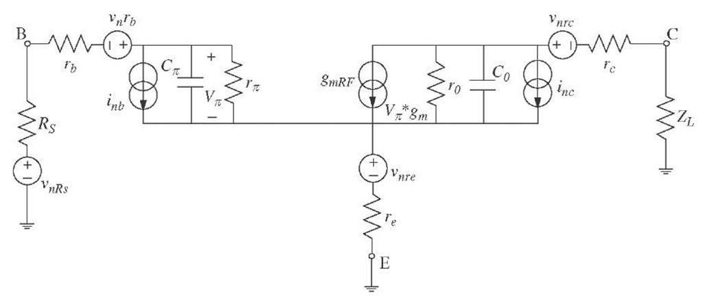
Noise Figure in Gilbert Mixers The main contributor to the noise figure in Gilbert mixers is the amplification stage, due to the fact that the signal has already been amplified afterwards and, applying Friis equation [Lee98], the noise added to the signal after amplification has less importance. To get an idea of the amount of noise added in this stage, each transistor in the differential pair is substituted for its quasi-linear noise model [Xavier97], which can be used at frequencies below 6GHz (see Figure 3-12).
In Figure 3-12, resistances![]() generate thermal noise shown in Eq. 3-11:
generate thermal noise shown in Eq. 3-11:
where k is Boltzmann’s constant, T is temperature, and r is the resistance value![]()
Base and collector currents![]() generate shot noise shown in Eq. 3-12:
generate shot noise shown in Eq. 3-12:
where![]() is the heterojunction bipolar transistor (HBT) transconduc-tance.
is the heterojunction bipolar transistor (HBT) transconduc-tance.
Figure 3-12 Hybrid n noise model
Base current![]() also generates flicker noise:
also generates flicker noise:
where q is the electronic charge and equals to![]() is the corner frequency and f is the frequency of interest. The flicker noise defined by Eq. 3-13 becomes dominant at frequencies below the corner, f1 value, and can be neglected above a few kilohertz.
is the corner frequency and f is the frequency of interest. The flicker noise defined by Eq. 3-13 becomes dominant at frequencies below the corner, f1 value, and can be neglected above a few kilohertz.
As can be seen in Figure 3-12, noise generators must be added: two current sources that represent the shot noise of the collector and base currents, and four voltage sources that represent the noise generated by the source resistance![]() parasitic base, emitter, and collector resistances
parasitic base, emitter, and collector resistances![]() Transferring all these sources to the input yields the model shown in Figure 3-13.
Transferring all these sources to the input yields the model shown in Figure 3-13.
In Figure 3-13,![]() is the noise generated within the source and
is the noise generated within the source and![]() is the noise of the mixer converted to a voltage source at the input. The different noise sources included in
is the noise of the mixer converted to a voltage source at the input. The different noise sources included in![]() are shown in Eq. 3-14:
are shown in Eq. 3-14:
where![]() is the thermal noise of parasitic resistances,
is the thermal noise of parasitic resistances,![]() is the base-emitter shot noise, and
is the base-emitter shot noise, and![]() is the collector emitter shot noise.
is the collector emitter shot noise.
Thermal noise of parasitic base and emitter resistances is shown in Eq. 3-15:
The thermal noise of the collector resistor is disregarded because the noise of rc is typically 105 times lower than collector-emitter shot noise [Xavier97].
Base-emitter shot noise is converted to a voltage noise source in series with the source resistor by applying the Thevenin conversion as shown in Eq. 3-16:
where Zn is the base impedance.
Figure 3-13 Noise model of transistor
The voltage source associated to the collector-emitter shot noise is shown in Eq. 3-17:
where![]() is the parallel of
is the parallel of![]() in Figure 3-12.
in Figure 3-12.
The noise figure expression of a device can be derived from the ratio between the total noise at the output to the noise of the source as shown in Eq. 3-18:
where![]() is the noise at the input of the device and
is the noise at the input of the device and![]() is the noise of the device itself.
is the noise of the device itself.
The noise figure expression is obtained by substituting Eq. 3-15, Eq. 3-16, and Eq. 3-17 in Eq. 3-14 and the last part of Eq. 3-8:
![]() are time-dependent variables because the modeling of the first stage of the mixer has been based on a small signal model of the transistor in the previous calculation. As the mixer is not a linear device,
are time-dependent variables because the modeling of the first stage of the mixer has been based on a small signal model of the transistor in the previous calculation. As the mixer is not a linear device, ![]() are not constant values. In [Xavier97], a model used to predict the noise figure of the HBT mixer is presented by splitting the influence of LO harmonics in the noise figure:
are not constant values. In [Xavier97], a model used to predict the noise figure of the HBT mixer is presented by splitting the influence of LO harmonics in the noise figure:
where the rows of Eq. 3-20 are the noise contribution from RF, DC, and image frequencies to IF output, respectively. All three rows have a similar structure: thermal noise from resistances, base shot noise contribution, and collector shot noise contribution, which are the elements multiplied by (1/g;).
Influence of Mixer Design on the Noise Figure Two main parameters that influence the noise figure of the differential pair and that must be taken into account when designing a mixer can be distinguished when analysing Eq. 3-20.
The base and emitter resistances![]() are the only parameters of the transistors that affect thermal noise and that can be modified by the designer. To reduce the noise generated by
are the only parameters of the transistors that affect thermal noise and that can be modified by the designer. To reduce the noise generated by![]() the number of base-emitter contacts and the emitter area must be as high and large as possible. However, the possible emitter area is limited due to parasitic capacitance
the number of base-emitter contacts and the emitter area must be as high and large as possible. However, the possible emitter area is limited due to parasitic capacitance![]() which is proportional to the emitter area. This capacitance affects impedance Z in Eq. 3-20. Therefore, depending on the RF frequency, a balance must be struck between reducing thermal noise and reducing gain, which creates a rise in the noise figure due to the higher influence of noise from consequent stages.
which is proportional to the emitter area. This capacitance affects impedance Z in Eq. 3-20. Therefore, depending on the RF frequency, a balance must be struck between reducing thermal noise and reducing gain, which creates a rise in the noise figure due to the higher influence of noise from consequent stages.
The transconductance![]() is directly proportional to the collector current
is directly proportional to the collector current![]() and this current is set when polarizing the mixer. If the transistor parameter b is high, the base shot noise contribution can be neglected and IC should be increased. However, if b, which is frequency dependant (as seen in Eq. 3-21) is not high enough, then shot noise of Ib influences the noise figure and IC should be reduced. The high-frequency small signal current gain [Gray84] is:
and this current is set when polarizing the mixer. If the transistor parameter b is high, the base shot noise contribution can be neglected and IC should be increased. However, if b, which is frequency dependant (as seen in Eq. 3-21) is not high enough, then shot noise of Ib influences the noise figure and IC should be reduced. The high-frequency small signal current gain [Gray84] is:
where![]() is the base-emitter parasitic capacitance and
is the base-emitter parasitic capacitance and![]() is the base-collector parasitic capacitance,
is the base-collector parasitic capacitance,![]() is the low frequency current gain and
is the low frequency current gain and ![]() the transconductance of the transistor.
the transconductance of the transistor.
Another consideration can be made from Eq. 3-20: The noise contribution of the second and third row can be minimised by filtering image and IF frequencies.
Influence of LO Power on the Noise Figure Once the mixer has been fabricated, there is a way to influence the noise figure, as can be seen in Eq. 3-20. The LO signal has great influence on the noise figure primarily because gm is directly proportional to LO power. In addition, the LO signal has additional influence on mixer noise: If the switching of the four transistors in the mixer core had been ideal (see Figure 3-11), then only two transistors would have been constantly conducting and only two transistors would have been generating noise. However, there are small intervals when all four transistors are switched on simultaneously. The length of this interval depends on the LO signal, specifically its voltage level and shape.
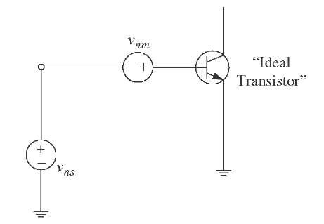
Linearity in Gilbert Mixers Gilbert mixer linearity depends mainly on its first stage, which transforms the voltage input signal into a balanced current. This function is carried out by the differential input pair that makes up the amplification stage. Its behaviour can be defined by a hyperbolic tangent function presented in Eq. 3-7 and included in Eq. 3-22.
In section 3.3.2.1 in Eq. 3-10, a linear conversion has been considered by equating tanh(x) with x, assuming that the input signal is a small one. However, when analysing mixer linearity, this assumption cannot be made because high input signals are used to test the mixer.
To obtain varying output harmonics, the tanh(x) function is approximated by its Taylor series as shown in Eq. 3-23:
If the input signal of the mixer is a two-tone signal, then it can be expressed as shown in Eq. 3-24:
where frequency![]() is close to frequency
is close to frequency![]() and A is the signal amplitude. The output signal is obtained by substituting Eq. 3-23 in Eq. 3-22. This is shown in Eq. 3-25:
and A is the signal amplitude. The output signal is obtained by substituting Eq. 3-23 in Eq. 3-22. This is shown in Eq. 3-25:
Linearity is measured through the IP3 parameter, which is the theoretical point where output components at![]() have the same amplitudes as those at
have the same amplitudes as those at![]() If input amplitude A is small enough to guarantee that
If input amplitude A is small enough to guarantee that![]() [Razavi97], then the IP3 point is given by Eq. 3-26:
[Razavi97], then the IP3 point is given by Eq. 3-26:
where![]() is the normalized input signal amplitude at IP3 point as shown in Eq. 3-27 and output IP3 is given by
is the normalized input signal amplitude at IP3 point as shown in Eq. 3-27 and output IP3 is given by![]()
In the input stage of a Gilbert cell, which is a differential pair, the![]() and
and![]() coefficients can be approximated by
coefficients can be approximated by![]()
![]() this means inputs up to ± 28.6mV for a bipolar differential pair operating at T = 300K. If the input signal amplitude is the maximum signal, 28.6mV, which corresponds to -11.84dBm for a 50Q input impedance, then the maximum input IP3 is as shown in Eq. 3-28:
this means inputs up to ± 28.6mV for a bipolar differential pair operating at T = 300K. If the input signal amplitude is the maximum signal, 28.6mV, which corresponds to -11.84dBm for a 50Q input impedance, then the maximum input IP3 is as shown in Eq. 3-28:
As can be seen in previous equations, Gilbert cell linearity can be approximated by a mathematical function that is not dependent on the values of the elements that form the circuit (transistors, resistors, etc.). Theoretically, the HBT pair in the amplification stage has a linearity limit near -5dBm. This is the maximum IP3 value obtained in a Gilbert cell, but this value can fall if the layout of the circuit is not carefully designed or perfect switching is not achieved. To obtain the maximum IP3 value, a design must follow these recommendations:
■ The switches in the mixer core should be made of small transistors, reducing base-emitter capacitance of switches and decreasing transition time. Linearity is improved because third-order intermodulation currents are generated only during transitions[Maas87].
■ Layout techniques such as common centroid should be used to achieve equal branches in the Gilbert cell.
■ The LO signal in the mixer core (see Figure 3-11) greatly influences linearity. It must drive enough power to quickly switch transistors within minimum transition time. However, an excess of power may charge the Cbe parasitic capacitor of transistors in the mixer core, producing undesired current peaks[Lee98].
Local Oscillator Isolation Local oscillator isolation, which depends on differential structure, is increased by assuring symmetry between the two sides of the differential Gilbert cell.
Linearising Techniques The only way to increase linearity is by modifying the value of the parameters included in Eq. 3-22. There are two methods widely used to linearise Gilbert cells: the inclusion of emitter degeneration [Gray84] and the use of a class-AB input stage to replace the HBT differential pair from the amplification stage[Gilbert00].
Emitter degeneration consists of including emitter resistors in the transistor pair from the RF stage. This is a very popular way to extend the linear range of operation. The improvement factor in the differential pair is approximately equal to IRe, with Ie and Re representing the emitter current and the resistor value, respectively. However, the use of emitter degeneration to improve linearity involves some consequences in gain and noise:
■ Voltage gain is reduced by approximately the same factor by which the input range is increased.
■ A new contributor is added to the voltage noise defined by Eq. 3-29:
which is the thermal noise resulting from emitter degeneration. In addition, because of voltage gain reduction in the differential input stage, the contributions to noise from following stages become more significant.
There are two kinds of degeneration that can be included in the emitter: resistive or inductive. Resistive degeneration is used when the RF signal is a low frequency or a wideband signal and shows a lower gain than the latter. Inductive degeneration is used with high frequency and narrowband signals.
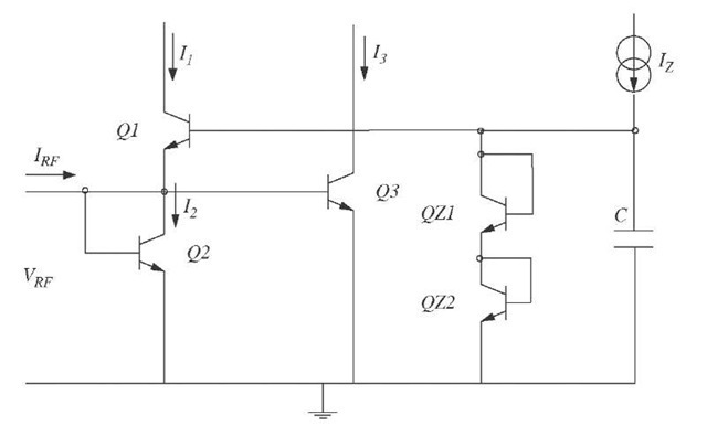
The bisymmetric class-AB topology based on translinear principles is a linearising technique that has no inherent gain compression [Gilbert00]. The input stage diagram is shown in Figure 3-14.
In this input stage, the relationship between IRF and the difference between I1 and I3 is shown in Eq. 3-30:
resulting in a linear operation, provided that the input signal is a current.
This stage has several points that must be taken into account when designing a mixer:
■ The input resistance of this stage is:
Figure 3-14 Simplified class-AB input stage
From Eq. 3-31, it can be seen that a very low value of I1 should be used to obtain a 50Q input resistance. However, this current value would result in poor gain and consequently higher noise.
■ The mixer gain associated with this input stage is:
When comparing Eq. 3-32 with the gain of the differential pair in Eq. 3-10, it can be seen that the gain in mixers employing class-AB as the input stage is twice that obtained in mixers with a differential pair in the input stage. However, in class-AB, the collector current Ic is lower in order to facilitate 50Q matching, resulting in lower gmRF.
■ The noise figure equation for mixers that use class-AB as the input stage is quite similar to the noise figure in mixers with Gilbert cells. Nonetheless, it includes some differences:
■ There are three transistors in the input stage, so there are three additional noisy current sources associated with shot noise from Ic and Ib.
■ The voltage gain is not high enough and the noise from the mixer core and the buffer influences the mixer’s global noise figure.
When AB topology does not completely meet linearity requirements, it is sometimes possible to combine both methods and to include emitter degeneration in all three transistors of the class-AB stage.
