Considering the technical requirements defined in the previous topic as the starting point, this topic will explain in detail the design of every block of the radio frequency (RF) front-end. To accomplish a design that fulfils specifications, the design is verified by means of the electrical schematic simulations, layout of the different components of the electrical schematic and post-layout simulations considering additional effects introduced by tracks, pads, such as stray capacitances , stray resistances carried out by RF engineers. Circuit design considerations, as well as the results of post-layout simulations for all the blocks of the front-end, are presented in this topic. The receiver chain and the phase-locked loop (PLL) are described separately. Moreover, the control logic, the PADs, and the floor planning of the RFIC are also presented. The design has been fabricated with a 0.35|im SiGe process, with four metal layers, two polysilicon layers, and a high-resistivity polysilicon layer (AMS-SiGe 0.35|im-BYS) to reduce both cost and power consumption.
Receiver Architecture
Figure 3-1 shows the proposed low-IF architecture for the combined GPS/Galileo front-end.This architecture, compared to Zero-IF, is insensitive to DC offsets and flicker noise. In Zero-IF receivers, DC-offset compensation is a severe problem since most GPS C/A-code signal energy is DC. The main drawback of a low-IF architecture is its limited image rejection. This can be improved when the frequency plan of the entire receiver is carefully designed. In the implemented receiver, the combined GPS/Galileo L1 band signal is down-converted to a low IF of 20.42MHz, causing the image signal to be rejected by the RF SAW filter. The obtained image rejection ratio is more than 40dB. When sampling the IF signal at 16.638MHz, the A/D converter also down-converts the incoming signal to a second IF of4.092MHz. Signal detection is then performed digitally on a second chip that contains all the digital processing and controlling parts of the receiver.
Figure 3-1 Block diagram of receiver
The PLL also allows for the choice of an LO frequency that down-converts the incoming RF signal directly to an IF of 4.092MHz. For this choice, the image lies in the GPS/Galileo L1 band and mainly consists of thermal noise.
Choosing the gain of the various blocks of the receiver is always a trade-off. A high-gain low-noise amplifier (LNA) will help to reduce Noise Figure (NF) by minimising mixer contribution, but at the expense of higher power consumption in this block. A low-gain LNA may improve linearity and power consumption, but would require a low-noise mixer. Such a mixer would consume a great deal of power. In other words, a low-gain LNA combined with a low-noise mixer may not offer a significant advantage in total power consumption over a high-gain LNA combined with a mixer with higher NF. Therefore, as shown in the previous topic, a relatively high-gain receiver configuration has been chosen. Figure 3-2 shows the resulting receiver specifications with gains, NF, and IIP3 given below each block. Front-end linearity is not an issue, since the received Galileo and GPS signals are very low power and relatively constant. Therefore, linearity specifications are dictated by the required system’s ability to perform in the presence of external interfering signals.
The total SSB noise figure, referring to the input of the on chip LNA, is 2.8dB, which is adequate for high-sensitivity applications.
The front-end bandwidth is approximately 6MHz, which comprises the two main lobes of the Galileo BOC(1,1) signal as well as the main lobe of the GPS C/A-code with its two side lobes. The C/N0 correlation loss caused by front-end filtering is less than 0.7dB for both signals.
Finally, the second IF signal is converted to digital signal with a 1bit A/D converter. Using a 1bit converter results in slightly degraded performance compared to that of multibit converter, but it allows the design of a simpler, lower-power receiver without automatic gain control.
Figure 3-2 Receiver specifications
Low-Noise Amplifier
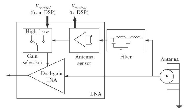
A dual-mode LNA with an integrated antenna sensor has been designed. The two LNA modes are comprised of a high-gain mode for a passive antenna and a low-gain mode for an active antenna, enabling the receiver to sense the presence of a passive or active antenna and avoid the risk of early receiver overloading due to unwanted interference signals.
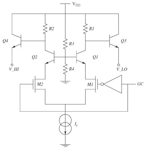
As shown in Figure 3-3, the low-noise amplifier consists of three subsystems: the core of the LNA, the antenna sensor circuit, and the gain selection stage.
LNA Core
The aim of the LNA is to amplify the low-power input signal received by the antenna while degrading the C/N0 as little as possible. Providing an input and output impedance of 50Q is also a critical requirement of the LNA. In the case of the input impedance, it serves as a way to match the antenna impedance, where, in the case of the output impedance, it helps to avoid an undesired degradation of preceding SAW filter characteristics (insertion loss, pass band ripple, etc.) due to mismatched impedances.
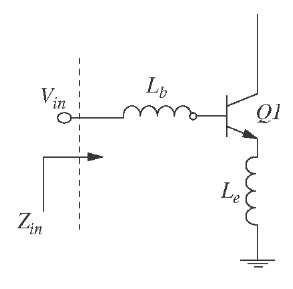
The 50Q input impedance can be achieved by adding an inductance in series with the emitter of the input transistor to degenerate the common emitter amplifier, as shown in Figure 3-4. This is the most popular LNA topology because it simultaneously achieves low-noise, high-gain, and input impedance matching compatible with a narrow frequency band.
Figure 3-3 LNA building blocks
Figure 3-4 Common emitter amplifier with emitter degeneration
Figure 3-5 shows the small signal equivalent circuit of the input transistor. Excluding the base-collector capacitance, the base emitter, and the emitter resistors, the input impedance of the amplifier can be illustrated as shown in Eq. 3-1.
It should be noted that there is a resistive component in the input impedance. To reach a resistive input impedance of![]() at the operating frequency, one can choose the value of
at the operating frequency, one can choose the value of![]() such that _ is resonated at the operating frequency with
such that _ is resonated at the operating frequency with![]() equal to
equal to![]() Eq. 3-2 and Eq. 3-3 are then solved, resulting in an input impedance of 50Q.
Eq. 3-2 and Eq. 3-3 are then solved, resulting in an input impedance of 50Q.
Figure 3-5 Small equivalent circuit of the SiGe input transistor
One of the most appealing advantages of this topology is that most of the resistive components of the input impedance are noiseless because they are synthesised with an inductor, unlike other techniques where a noisy resistor is added to the signal path to provide 50Q termination resistance[Shaeffer97]. This explains the low-noise performance and popularity of the inductively degenerated common emitter LNA.
When calculating the effective small-signal transconductance of the input transistor, it is worth noticing that the input-matching circuit is a pure series RLC resonant circuit. At resonance, the voltage across is enhanced by Q amount of times, where Q is the quality factor of the input-matching RLC network. In other words, the Q enhancement mechanism provides a free gain of Q for both the input signal and the noise from the source resistance RS. The added gain from the input-matching circuit helps to mitigate the effect of the channel’s thermal noise, which accounts for the superior noise performance of the common-source LNA with inductive degeneration. Furthermore, the effective transconductance is also enhanced by a factor of Q as shown in Eq. 3-4[Li04]:
If the input is matched to![]() as shown in Eq. 3-5, transconductance results in:
as shown in Eq. 3-5, transconductance results in:
![]() is usually equal to
is usually equal to![]() in an RF system. It is worth noting that the effective transconductance
in an RF system. It is worth noting that the effective transconductance![]() is only related to the ratio of
is only related to the ratio of![]() and is not dependent on small-signal transconductance
and is not dependent on small-signal transconductance![]() However, parasitic input path capacitance and base-collector capacitance are also present. The base-collector capacitance
However, parasitic input path capacitance and base-collector capacitance are also present. The base-collector capacitance![]() provides a feedthrough path from input to output and thus decreases the reverse isolation. In addition, its interaction with the inductive load at the output introduces a negative resistance at the input, which causes stability concerns. Furthermore, the Miller effect of
provides a feedthrough path from input to output and thus decreases the reverse isolation. In addition, its interaction with the inductive load at the output introduces a negative resistance at the input, which causes stability concerns. Furthermore, the Miller effect of![]() and the
and the![]() associated with the bond pad provides a shunt current branch at the input, which further complicates input matching. One can add a cascade stage to mitigate the Miller effect of
associated with the bond pad provides a shunt current branch at the input, which further complicates input matching. One can add a cascade stage to mitigate the Miller effect of ![]() and improve the reverse isolation. However, this results in additional noise from the cascode transistor, which degrades the noise figure if not optimally designed[Li04].
and improve the reverse isolation. However, this results in additional noise from the cascode transistor, which degrades the noise figure if not optimally designed[Li04].
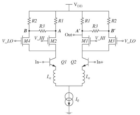
The core of the implemented cascoded LNA with the resistor chain [Fong99][Garaa01] (used to perform gain switching) is shown in Figure 3-6. Transistors Q1 and Q2 and degeneration on-chip inductors Le (900pH) form the previously mentioned common emitter transconductance stage[Shaeffer97]. These transistors have multiple-base contacts in order to minimise the noise introduced by the base resistance![]() thereby reducing the NF (Eq. 3-6).
thereby reducing the NF (Eq. 3-6).
Figure 3-6 LNA core
where Rs is the source resistance and IC is the collector current. Base shot noise is not included in Eq. 3-6 as a current noise source [Razavi97]. As mentioned before, the degenerating inductors allow conjugate input impedance matching and improve circuit linearity.
As the RF input signal is single-ended (In+), In- is consequently grounded through a 22pF capacitor. The use of a single-ended input within a differential-like architecture reduces the number of external components (such as a balun) and mitigates the effect of parasitic ground and VDD bondwire parasitics on LNA performance. The amplified RF current, by means of Q1 and Q2 transistors, flows through both Ml and M2 cascode transistors to reach the LNA output in high-gain mode. In low-gain mode, the amplified RF current flows through both M3 and M4 cascode transistors before being split by resistor chains (R1 and R2), while Ml and M2 are switched off during the gain-switching stage. The gain step between the two modes of operations depends (during initial approximation) on the resistor ratio R2:R1. The advantage of this kind of configuration is that the gain step does not depend on how accurately the resistors match in terms of their absolute value, but on their ratio R2:R1. Therefore, the gain step can be accurately controlled.
In the high-gain mode, the gate voltage of the transistors is set to the appropriate values to switch on Ml and M2 and switch off M3 and M4. Hence, both transistors Ml and M2 act as cascode transistors in the transconductance stage. LNA gain is the highest in this mode because the amplified RF current is injected into nodes A and A!, which have the highest resistance of the resistor chains.
In low-gain mode, M3 and M4 act as cascode transistors while Ml and M2 remain switched off. The LNA gain is the lowest because the current from the transconductance stage is injected into nodes B and B’, which have the lowest resistance of the resistor chain.
An emitter follower stage is used at the LNA output to perform on-chip output impedance matching. It also contributes to the system input/output isolation, therefore improving amplifier stability.
Antenna Sensor and Gain Selection Circuitry
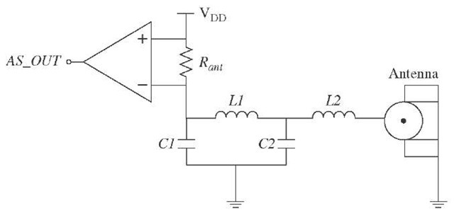
In order to select high gain (for passive antennas) or low gain (for active antennas) for the LNA, the system is able to detect automatically whether the antenna is active or passive by means of the antenna sensor (see Figure 3-7)
The antenna sensor detects the antenna type and sets the AS_OUT pin as shown in Table 3-1.
The operation of the sensor is very simple and can be explained in two steps:
■ An active antenna consumes a current that flows through Rant. It will generate a voltage difference between Rant and the AS_OUT pin will be "high."
■ A passive antenna does not consume any current, so there is not a voltage difference at Rant, resulting in the AS_OUT pin being "low."
Figure 3-7 Antenna sensor circuit
TABLE 3-1 AS_OUT pin, antenna sensor
|
Antenna Type |
AS_OUT Logic Value |
|
passive |
low |
|
active |
high |
The control signal AS_OUT is buffered out to the digital control with information about the antenna type, which allows the digital processing unit (along with information about the C/N0) to establish the gain requirement. The digital processing unit then sets the control voltage GC back to the gain selection stage of the LNA.
The gain selection circuit (see Figure 3-8) sets the bias voltage, controlled by the GC pin (see Table 3-2), to make the LNA work in high-gain or low-gain mode.
The values of the V_HI and V_LO nodes set the gain of the LNA by changing the bias voltage of the core’s cascode transistors. The ON and OFF voltages have been defined as 3.3V and 1.1V, respectively. In high-gain mode, the GC will be low and Ml will be ON and M2 OFF, establishing 3.3V for V_HI and 1.1V for V_LO, set by the voltage difference at Rl.
Figure 3-8 Gain selection circuit
TABLE 3-2 Gain selection by means of the Gain Control (GC) pin states
|
GC Logic Value |
Gain |
|
low |
max |
|
high |
min |


