Information Technology Reference
In-Depth Information
2.1
Overview
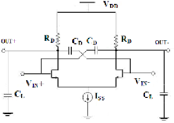
Figure 1 shows the basic CML buffer. It consists of a differential pair with two
NMOS transistors, which act as switches. When the differential input (V
IN+
- V
IN-
)
varies from 0 to V
DD
, the output in each branch varies from V
DD
to (V
DD
- I
SS
R
D
/2),
or vice versa. Thus, the differential output voltage swing achieved is I
ss
R
D.
Low
switching noise, higher common mode rejection due to differential architecture & low
swing signaling make CML an attractive choice for high frequency applications.
Fig. 1.
Conventional CML Buffer
2.2
Limitations of a CML Buffer at High Frequencies
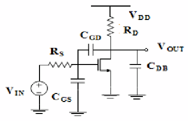
Figure 2 shows the half circuit diagram of the CML buffer which is a standard
common-source amplifier.
Fig. 2.
Half circuit of CML buffer buffer
The dominant pole (ω
p1
), and the first non-dominant pole (ω
p2
) of this circuit are
given approximately by
ω
p1
= 1 / [R
S
(1 + g
m
R
D
)C
GD
+ R
S
C
GS
+ R
D(
C
GD
+ C
DB
)] . (1)