Information Technology Reference
In-Depth Information
Strong fringe coupling on the undoped underlap region is observed by introducing
high-
k
dielectric spacer. This helps in arranging the inversion charge carriers for
which the extra parasitic series resistance is reduced that increases
I
on
. It is clear from
Fig. 3 that, as the spacer-
k
increases, there is an improvement in device performance
due to strong electric field coupling between a gate terminal and the underlap regions.
Both, the
I
on
and the
I
on
/I
off
parameter increases with an increasing spacer dielectric
value due to an increased GFIBL effect [8]. The
I
on
/I
off
ratio initially increases with
the increase in underlap (Fig. 3(c)) and then becomes saturates after 4nm.
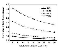
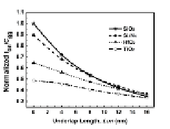
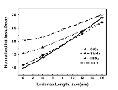
Fig. 4.
Variation of the normalized (a) total gate capacitance, (b) drive current-to-total gate
capacitance ratio (
I
on
/
C
GG
) and (c) the gate intrinsic delay for different spacer with varying
underlap length (
L
un
)
The variation in total gate capacitance (
C
GG
) with
L
un
for different spacer materials
are shown in Fig. 4(a). The gate capacitance is normalized with the reference device
with zero-underlap having low-
k
(SiO
2
) spacer material. Clearly, the
C
GG
decreases with
increasing underlap. Since, both the
C
GG
and the
I
on
decrease with the underlap there-
fore, performance will also change depending on their rate of decrease. The
I
on
/
C
GG
must be enough high to substantially reduce the delay. For zero underlap, the
I
on
/
C
GG
asset values decrease by introducing high-
k
spacers. Furthermore, it decreases with
increasing underlap and for
L
un
=16nm underlap length; the
I
on
/
C
GG
is at minimum and
same for different spacer materials. Fig. 4(c) indicates that the intrinsic delay through
the circuit with high underlap will be more than that of a non-underlap case.
4
SRAM Performance Projections
This section provides the cell operation and methodology used in the underlap
FinFET
SRAM cell. The schematic of the tied-gate 6-T SRAM cell is presented in Fig. 5(a). The
thick red and blue lines represent the large line capacitances associated with the word-
line (WL) and bit lines (BL and BLB), respectively. The PMOS pull-up transistors (PU
L
and PU
R
) and NMOS access transistors (PA
L
and PA
R
) are of minimum size to set a
pull-up ratio of one. Analyses are drawn based on the simulations performed for cell-
ratio two, by using double-fin of the pull-down transistors (PD
L
and PD
R
).
During the hold mode, node Q and QB store logic "1" and "0", respectively and
word-line is off. Hold-SNM defines the stability in retention to preserve the stored
data. During a read operation, the word-line access transistors are ON after the bit
lines are precharged. The read-SNM is the metric used in read mode for reliable oper-
ation [9]. For higher read stability, access transistor strength must be low. Read access