Information Technology Reference
In-Depth Information
Table 1.
ITRS projections for high performance device in year 2017
Device Parameters
Abbreviations
ITRS Projections Value
L
G
Physical Gate Length
14 nm
Eq. Oxide Thickness
EOT
0.72 nm
Fin Thickness
T
si
9.4 nm
Supply Voltage
V
DD
0.75 V
1×10
16
cm
-3
1×10
20
cm
-3
220 mV
Channel Doping
Source/Drain Doping
Threshold Voltage
N
A
N
D
V
tsat
3
Device Characteristics with Underlap Length
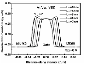
The conduction band profile across the channel with an increasing underlap length as
shown in Fig. 2(a) and 2(b) at
V
DS
=0, and
V
DS
=
V
DD
,
respectively when
V
GS
=
V
DD
. Fig.
2(a) clearly depicts that the underlap barrier increases and hence
R
S/D
with an increas-
ing underlap length. It is also observed that the G-S/D underlap barrier is higher than
the channel region barrier at
V
DS
=0V. With an increasing drain potential, the underlap
barrier on the drain side reduces without affecting much the source side (G/S) under-
lap barrier as shown in Fig. 2(b). This source-side underlap barrier restricts the carri-
ers to flow from source to drain. Introduction of the high-
k
spacer reduces underlap
barriers to increased fringe coupling between gate and underlap region known as gate
fringe induced barrier lowering (GFIBL) [8]. Therefore, the incorporation of optimal
G-S/D underlap in nanoscale FinFETs is essential.
Fig. 2.
Conduction band profile along the channel with increasing underlap length (a) at
V
DS
=0,
and (b)
V
DS
=
V
DD
,
when
V
GS
=
V
DD
Fig. 3.
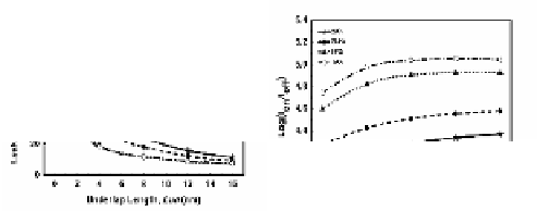
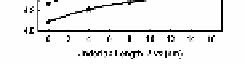
Variation of (a) drive-current, (b) leakage current, and (c) drive-to-leakage current ratio
for different spacer with varying underlap length (
L
un
)