Information Technology Reference
In-Depth Information
adaptive circuit techniques like source biasing and dynamic VDD have been proposed
[6]. Different types of Single ended and differential operating bitcells have been
proposed. For achieving improved read stability, different bitcell configurations use an
extra sensing circuit for reading cell contents. Considering the fact that the stability of
the inverter pair should be improved for stable SRAM operation at low supply voltages,
Jaydeep P. Kulkarni et. al had proposed a Schmitt trigger based differential bitcell
having built-in feedback mechanism for improved process variation tolerance [7].
The rest of this paper is organised as follows. In Section 2 the operation of basic
SRAM cell, conflicting read vs. write design requirement and Schmitt trigger
principle for cross-coupled inverter pair are discussed. Section 3 describes proposed
SRAM bitcell. Section 4 covers the simulation results and paper concludes with
Section 5.
2
Conventional 6T SRAM Bitcell
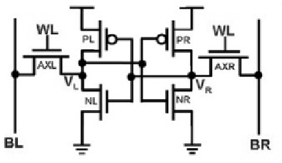
The basic static RAM cell is shown in Fig. 1. It consists of two cross-coupled
inverters and two access transistors. Four of the transistors are used to make a pair
of inverters - NOT gates, essentially. Each inverter requires a pair of transistors - if
the input is 0, then the p-type transistor will be on, and the n-type off. This will
connect the output to power, which is equal to logic 1. Otherwise, if the input is 1, the
output will be connected to ground, or logic 0.
Fig. 1.
Conventional symmetrical 6T bitcell
The two inverters are connected in a loop, with the output of one, the input of the
other. The access transistors are connected to the wordline at their respective gate
terminals, and the bitlines at their source/drain terminals. The wordline is used to
select the cell while the bitlines are used to perform read or write operations on the
cell. Internally, the cell holds the stored value on one side and its complement on the
other side.
This arrangement has two stable states: we interpret these two states can be
interpreted as 1 and 0. The other two transistors are used to control reading and
writing. To read the contents of the RAM cell, the
word
line (WL) is set high,