Information Technology Reference
In-Depth Information
4
Experimental Result of WCPG_in_PG
The technique of WCPG_in_PG is implemented taking dk27 benchmark circuit. The
circuit has been designed and simulated in CADENCE virtuoso spectre at 45 nm
TSMC technology. Supply voltage (VDD) is taken as 1V. Efficiency has been estab-
lished by comparing the results with the no power gating, FSM based power gating
(PG) and within_clock_ power_gating technique (WCPG).
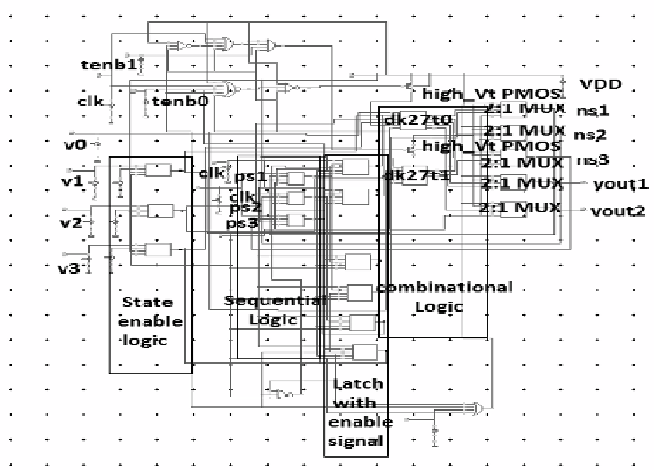
After creating symbols of all the gates they are integrated to build the complete
schematic of dk27 circuit without WCPG_in_PG and dk27 circuit with
WCPG_in_PG
design (Fig. 2).
Leakage power saving is influenced by shutting down power supply of the inactive
block and operational frequency. As the clock period is larger, the idle time of the
combinational logic becomes more because the difference between evaluation time and
clock period increases and hence, greater leakage power saving is achieved. During
evaluation time transitions occur, whereas, no transitions occur during idle time. Leak-
age power and average power are calculated for different input combination at
0.1MHz, 0.05MHz, 0.03MHz, 0.025MHz frequency and also the power results of
WCPG are compared with the results of PG and no power gating(no PG) technique at
0.1 MHz frequency. In this WCPG_in_PG
technique leakage power is calculated at the
positive part of clock cycle. Depending on MSB bit at a certain time one sub-FSM is in
power gated mode at both edge of clock and other active sub-FSM is in power gated
mode at positive edge of clock and it is in active mode at negative edge of clock.
Fig. 2.
Schematic of
dk27 circuit with WCPG_in_PG
designed in CADENCE virtuoso spectre