Information Technology Reference
In-Depth Information
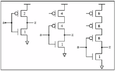
Fig. 6.
NOR gate matching unit inverter
Proceeding in a very similar way, the NOR gate can have a PMOS to NMOS tran-
sistor ratio of
ʳ
; the NMOS to PMOS conductivity is
ʼ
; and the value for K
P
of the
NOR gates need not be equal to the number of series PMOS transistors. A 2-input
NOR gate with the equivalent drive of an inverter with PMOS to NMOS is
ʳ
:1 has
PMOS to NMOS as K
P
·
ʳ
:1. This matches the conductivity of the NMOS transistor of
the reference inverter. Thus the falling logical effort is;
(1
+
K
γ
)
(11)
g
=
P
d
(1
+
μ
)
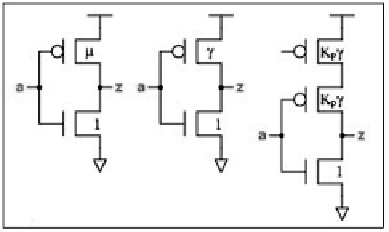
Fig. 7.
NOR gate for shortest falling
For the rising logical effort, we scale the PMOS transistor of the equivalent inverter to
PMOS equal to
ʼ
. The series PMOS transistors of the NOR gate are scaled to K
P
·
ʼ
.
Thus the rising logical effort is;
(
K
μμγ
μ
+
)
(12)
g
=
P
u
(1
+
)
The logical effort g is computed as:
1
2
(
K
γ
++
1
K
μ
+
μ γ
)
(13)
g
=
P
P
(1
+
μ
)