Information Technology Reference
In-Depth Information
the normal skewed gates, high skewed gates and low skewed gates. The validation for
minimum delay was done through simulation on a chain of inverters. We have also
compared our result with a chain of inverters which favors a particular transition.
2
Estimating Logical Effort and Sizing
The conductivity ratio between NMOS and PMOS transistors is defined as ʼ. The
value of ʼ is calculated by simulating an inverter for equal rise and fall time. By keep-
ing the width of NMOS to be constant and varying the PMOS width, a value of 2
approximately has been observed having equal rise and fall time. This becomes our
reference inverter for calculating logical effort.
The logical effort of a gate is denoted by g, and is the average of the rising logical
effort gu and the falling logical effort gd.
1
2
(1)
(
)
g
=
g
+
g
d
u
The falling logical effort of a gate is determined by setting the width of the NMOS
transistor to be equal to the reference inverter's, scaling the PMOS transistor size, and
using the ratio of the input capacitance. For an inverter, ratio of PMOS and NMOS
transistor is gamma (ʳ). We set the NMOS transistor size to be 1 and the PMOS tran-
sistor size to be ʳ. The falling logical effort is given by;
(
)
1
1
+
γ
μ
(2)
g
=
(
)
d
+
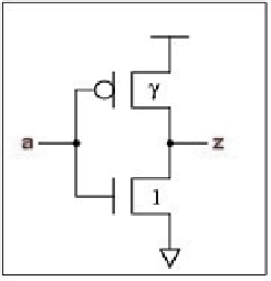
Fig. 1.
Inverter for shortest falling delay
For the rising logical effort, the PMOS transistor size is set equal to ʼ which means
that the NMOS transistor must be scaled down to ʼ/ʳ. This gives a rising logical effort
of:
(
)
μμγ
μ
+
(3)
g
=
u
(
)
1
+