Environmental Engineering Reference
In-Depth Information
CuInSe
2
CuInGaSe
2
Growth Voltage (V)
Cathodic potential (V)
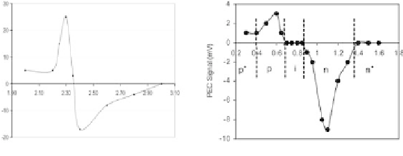
Figure 3.6
PEC signals observed for various samples of CuInSe
2
and
CuInGaSe
2
materials grown at different deposition voltages. Note the ability
to grow p
+
,p,i,n,andn
+
materials from the same electrolyte, simply by
varying the deposition voltage to alter material composition [16, 17].
junction diminishes and the positive PEC signal reduces to zero,
as shown by the curve AB. On the other hand, doping with Ga
by adding Ga
2
(SO
4
)
3
to the bath reduces the p-signal to zero
(AC) due to compensation and increases the n-signal (CD) because
of appropriate doping suitable for Schottky-type devices. Further
addition of Ga heavily dopes the material, causing the depletion
region to diminish and, hence, the n-signal to reduce to zero (DE).
This clearly demonstrates that ZnSe can easily be doped to produce
both n-type and p-type materials using the electrodeposition
technique.
Figure3.6showsexamplesofintrinsicdopingofsemiconductors
making use of their composition changes. Both CuInSe
2
[16] and
CuInGaSe
2
[17] layers show p-type conduction when the material
is rich in Cu at lower growth voltages. However, when the material
is grown at higher cathodic voltages, layers become rich in indium,
hence changing to an n-type material. The shape of the curve for
CuInGaSe
2
is slightly different due to the presence of Ga in the
bath.Thispropertyisextremelyimportantsincep-i-nstructurescan
be fabricated using one electrolyte simply by changing the growth
voltages of the material. For example, the p-i-n structure based
on CIGS could be grown by applying voltages at 0.60 V, 0.75 V,
and 1.10 V, in that order, for given time periods. Also, in the case