Environmental Engineering Reference
In-Depth Information
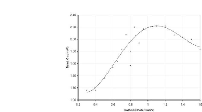
Figure 3.7
The variation of the energy bandgap between
∼
1.10 and
2.20 eV for electrodeposited CuInGaSe
2
layers grown as a function of
cathodic potential [17].
of development of graded bandgap multi-layer devices, this is an
excellent feature to exploit.
3.4.4
Observations in Optical Absorption Measurements
Optical absorption technique allows the determination of the
energy bandgap of semiconductors. Figure 3.7 shows the measured
bandgap values of CuInGaSe
2
layers electrodeposited as a function
of cathodic potential, and it is clear that the bandgaps can be
varied from 1.10 eV to
∼
2.20 eV by changing the deposition voltage
[17]. The 1.10 eV bandgap is very close to CuInSe
2
grown at
low cathodic voltages, and the bandgap increases as the cathodic
potential increases, due to attraction of more Ga into the deposited
layer. Again, this property can be used to develop graded bandgap
solar cell structures.
3.4.5
Observations in Photoluminescence
ZnSe layers grown by electrodeposition and MBE techniques have
been studied using photoluminescence under identical conditions
in order to compare the defect levels present in their forbidden