Information Technology Reference
In-Depth Information
D
D
D
0
FA
P
i
FA
A
i
B1
B0
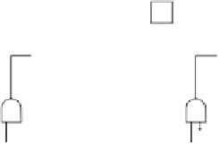
Figure
4.23.
Block schematic of bit-serial multiplier.
D-latches in this schematic are required for the proper operation of the device and
are not QCA zone latches. In order to map this design into a QCA circuit, we have
to realize that many more D-latches are introduced from the very nature of the
QCA circuit. The D-latch between the two adder blocks in the original schematic
(Fig. 4.23), is implemented in QCA by adding four additional clocking zones (one
clock cycle) along that path.
One of the inputs to the multiplier is serially connected across the multiplier
circuit; the other is constant and implemented using fixed polarization cells. The
schematic for this multiplier is shown in Figure 4.24. The overall latency for the
D3
D3
M
D1
D2
M
D1
D2
D0
M
D1
D2
M
D3
D0
M
D1
D2
M
D3
Pi
D0
D1
D2
D1
D1
D2
D0
D0
D2
D3
D0
D0
1
−
D3
D3
−
1
−
1
D2
D2
D2
D2
D1
D2
Ai
D3
D0
D1
D1
D1
B1
B0
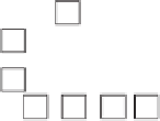
Figure
4.24.
Schematic of QCA bit-serial multiplier.


Search WWH ::

Custom Search