Information Technology Reference
In-Depth Information
P
i
Output is
LSB first
−
1.00
1.00
−
1.00
−
Ai
Input is LSB first
B1
B0
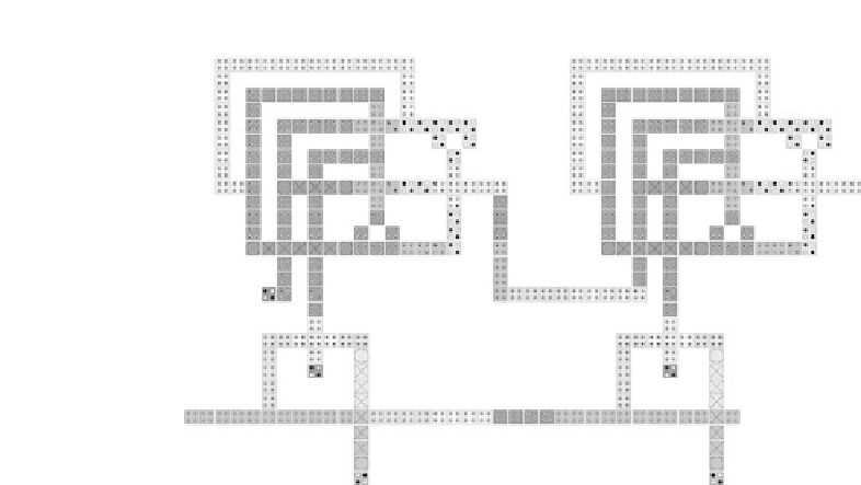
Figure
4.25.
Layout of QCA bit-serial multiplier.
multiplier is three clock cycles: one clock cycle inherent to each adder and one to
implement the latch between them.
The QCA layout for the multiplier is shown in Figure 4.25. The schematic is
drawn to match the layout as much as possible, and the multiplier can be easi-
ly scaled by adding full adder blocks and partial product generators. We have
experimented with designs as large as 32-bit using this layout. The size of the
multiplier grows linearly with the number of bits, making it efficient in area. The
latency also increases according to
L
¼
2n
1
;
where the latency, L, is measured in clock cycles, and n is the size of the multiplier
in input bits.
4.11.3. Memory
Zone clocking creates a shift register with each wire of clocked cells. However,
each cell is connected to a clock signal that will clear the cell contents once every
clock cycle. To correct for this loss of data, small loops can be used to retain
information and implement memory. The simplest memory loop consists of all
four clocking zones, enabling the information to continuously circulate in the
loop. A similar approach using continuous clocking has been proposed by Blair
et al. [30]. Figure 4.26 shows a QCA memory loop without any mechanism for
reading or writing information.


Search WWH ::

Custom Search