Hardware Reference
In-Depth Information
XA<19:18>
GAL16V8
EEPROM_CS
R/W
ECS
OE
SRAM_CS
WE1
WE0
A0
XA<17:14>
D[15:8]
D[7:0]
D[7:0]
WE
WE
OE
OE
AD[15:8]
2D [7:0]
K6R1008C1D
AT28C010
CS
ECS
1E
2E
CS
A[16:0]
A[16:0]
1Q0
HCS12DP256B
Q[13:1]
74ABT16373B
A[16:0]
A[16:0]
1OE
2OE
CS
CS
K6R1008C1D
AT28C010
OE
AD[7:0]
1D [7:0]
OE
D[7:0]
D[7:0]
WE
WE
D[7:0]
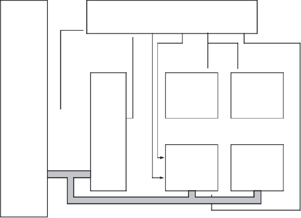
Figure 14.46
■
HCS12DP256B paged external memory example
Therefore, the complete address inputs A16, . . . , A0 to the memory chips become valid 20.5 ns
after the start of a bus cycle.
C
HIP
-S
ELECT
S
IGNALS
T
IMING
The ECS signal becomes valid 16 ns after the start of a bus cycle. XA19, . . . , XA18 are
valid 6 ns after the start of a bus cycle. The GAL16V8 has a propagation delay of 3.5 ns.
Therefore, the chip-select signals SRAM_CS and EEPROM_CS become valid 19.5 ns after the
start of a bus cycle. Because the HCS12 stops driving the XA19, XA18, and ECS signals 2 ns
after the end of a bus cycle, these two chip-select signals will become invalid 5.5 ns after the
end of a bus cycle.
W
RITE
-E
NABLE
S
IGNALS
T
IMING
Since WE1 and WE0 are a function of A0 and R/W and A0 is valid later than R/W, the valid
times of WE1 and WE0 are determined by A0. Since A0 is valid 20.5 ns after the start of a bus
cycle and the propagation delay of the GAL16V8 is 3.5 ns, WE1 and WE0 will become valid 24 ns
after the start of a bus cycle. The HCS12 deasserts the R/W signal 2 ns after the end of a bus cycle;
both the WE1 and WE0 signals become invalid 5.5 ns after the end of a write cycle.


Search WWH ::

Custom Search