Hardware Reference
In-Depth Information
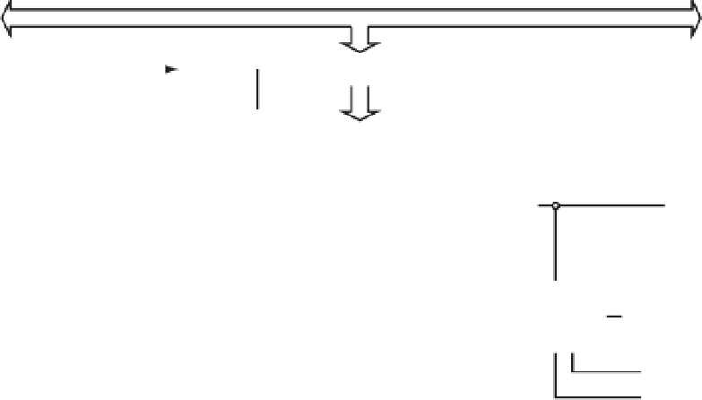
Internal bus
E-
clock
Baud divider
÷16
SCI data register
SBR12-SBR0
M
H8765
4
3210L
TxD
Loop
control
T8
To RxD
PE
PT
Parity
generation
Loops
RSRC
Transmitter control
TDRE
TIE
TE
SBK
TDRE interrupt request
TC
TCIE
TC interrupt request
Figure 9.11
■
SCI transmitter block diagram
start bit automatically goes into the most significant bit position. Hardware supports odd or
even parity. When parity is enabled, the most significant bit of the data character is the parity
bit. The transmit data register empty flag, TDRE, in the SCI
x
SR1 register becomes set when
the SCI data register transfers a byte to the transmit shift register. The TDRE flag indicates
that the SCI data register can accept new data from the internal data bus. If the transmit inter-
rupt enable bit, TIE, in the SCI
x
CR2 register is also set, the TDRE flag generates a transmit
interrupt request.
When the transmit shift register is not transmitting a frame, the TxD output signal goes
to the idle state, logic 1. If at any time software clears the TE bit in the SCI
x
CR2 register, the
TxD signal goes idle. If software clears the TE bit while a transmission is in progress, the frame
in the transmit shift register continues to shift out. To avoid accidentally cutting off the last
frame in a message, always wait for TDRE to go high after the last frame before clearing the
TE bit.
Use the following procedure if it is desirable to separate messages with preambles with
minimum idle line time:
1. Write the last byte of the first message to the transmit data register.
2. Wait for the TDRE flag to go high, indicating the transfer of the last frame to the
transmit shift register.
3. Queue a preamble by clearing and then setting the TE bit.
4. Write the first byte of the second message to the transmit data register.


Search WWH ::

Custom Search