Hardware Reference
In-Depth Information
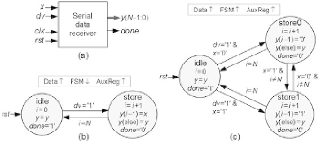
Figure 11.14
Serial data receiver. (a) Circuit ports. (b) Solution based on i gure 3.16c (FSM operating at the
negative clock edge). (c) Solution with all units operating at the same clock edge.
Two additional solutions are presented in i gure 11.14, this time using category 3
machines, both of Moore type and without timed transitions. The FSM of i gure 11.14b
was based directly on that of i gure 3.16c, with the timer (
t
) replaced with a pointer
(
i
). As indicated in the rectangle above the state machine, the data is updated at the
positive clock edge, which is also the edge that causes the storage of
i
and
y
in auxiliary
registers, whereas the FSM operates at the negative clock transition.
A i nal solution is presented in i gure 11.14c, operating with the default clocking
scheme (everybody operating at the same clock edge). In this case the i rst bit of
x
is
not lost because it is part of the transition conditions (observe the
idle-store0
and
idle-
store1
transitions, the i rst for
x
= '0', the second for
x
= '1').
11.7.8 Memory Interface
We want to develop a circuit for the memory interface of i gure 11.15a, which must
write data to an asynchronous SRAM chip. The only nonoperational input is
dv
(data
valid), and the outputs are
A
(address at which the data must be stored),
OEn
(output
enable, active low),
CEn
(chip enable, active low), and
WEn
(write enable, also active
low). The actual memory-write command, internal to the SRAM, normally corresponds
to the overlap between
CEn
and
WEn
. As in the previous example, this too is a simple
circuit, but it is important to understand how it can be modeled as a i nite state
machine.
Figure 11.15b shows a possible (conservative) memory-write sequence. All signals
are updated/produced at positive clock edges. As usual, a small propagation delay is
included between clock transitions and corresponding responses in order to portray
a more realistic situation. In this example it is assumed that writing occurs only while
dv
is high. When
dv
is raised, the circuit lowers
CEn
and
WEn
, causing
D0
to be