Hardware Reference
In-Depth Information
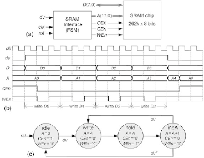
Figure 11.15
FSM implementing a memory-write procedure for an asynchronous SRAM. (a) Circuit ports. (b)
Illustrative timing diagram (note that here writing occurs while
dv
is high). (c) Corresponding
state machine.
stored at the initial memory address, after which
WEn
is raised, disabling further
writing. Each subsequent iteration consists of three clock cycles, during which the
memory address is updated and then another write-enable pulse (
WEn
= '0') is applied
to the circuit. When
dv
returns to '0', the address is reset to zero (or to any other
initial value). These operations can be done with
OEn
permanently high (thus not
shown).
A Moore-type state machine capable of implementing this sequence of events is
presented in i gure 11.15c, which is a direct translation of the timing diagram of i gure
11.15b. The address is updated in state
incA
, which increments the value of
A
. Note
the recursive expressions
A
=
A
and
A
=
A
+ 1, which characterize a category 3 FSM.
An example involving an actual SRAM chip is depicted in i gure 11.16. The SRAM
(IS61LV25616 device, from ISSI) is shown in i gure 11.16a. It can store 262 kwords of
16 bits each, hence requiring an 18-bit address bus,
A
(17:0), and a 16-bit data bus,
D
(15:0). It also contains i ve control signals, all active low, called
CEn
,
WEn
,
OEn
,
UBn
(upper byte enable), and
LBn
(lower byte enable).
A memory-write procedure based on this device's truth table and time parameters
is presented in the left half of i gure 11.16b. Note that it is less conservative than that
in i gure 11.15b (the end of the
WEn
pulse coincides with the beginning of a new