Information Technology Reference
In-Depth Information
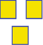
A(t−1)
REG
REG
IN1
A(t)
SUM
REG
IN2
A
ADDER
IN3
REG
SUM(t−1)
A)
Delay loop = N clock cycles
A(t−N)
IN1
A(t)
SUM
IN2
A
ADDER
IN3
SUM(t−N)
B)
Fig. 20.
Circuit example. The algorithm is
SUM
(
t
)=
A
(
t
)+
A
(
t −
1) +
SUM
(
t −
1).
(A) CMOS implementation. (B) NML implementation. An additional delay, under the
form of a wire loop, is used to map the additional delay on signal
A
.
input, but at the same time the previous input (
a0
) reaches the second adder
input because it is delayed of exactly N clock cycles. As a general rule, for
each additional delay of one clock cycle in the original circuit, an additional
delay of N clock cycles must be added to the correspondent wire in the NML
implementation.
Figure
21
shows the circuit simulation. In Fig.
21
(A) the CMOS implemen-
tation is depicted, while in Fig.
21
(B) the NML simulation, with the use of the
additional synchronization delay, is shown. The time scale is different because in
the CMOS implementation, one data is sent every clock cycle while in the NML
implementation one data is sent every N clock cycles, but the behavior is the
same. If the signal A is not correctly delayed the result is wrong, as can be seen
from Fig.
21
(C).


Search WWH ::

Custom Search