Information Technology Reference
In-Depth Information
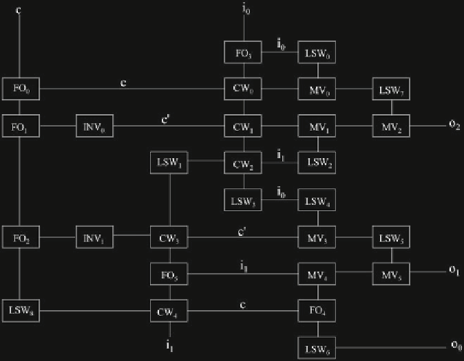
Fig. 19.
Modeling of QCA Layout of Fredkin Gate. FO represents the fanout QCA
device, LSW represents the L-shape wire, INV represents the QCA inverter, CW rep-
resents the crosswire and MV represents the majority voter
simulated for the presence of all possible single missing/additional cell defect in
MVs (majority voters), INVs (Inverters), FOs (fanouts), Crosswires (CWs) and
L-shape wires (LSWs). The design is simulated using the Verilog HDL simulator
in the presence of faults to determine the corresponding outputs.
We conducted exhaustive testing of the HDLQ model of the Fredkin gate
with 8 input patterns in the presence of all possible single missing/additional
cell defect. Testing of the Fredkin gate generates 28 unique fault patterns at the
output, as shown in Table
2
. In the fault patterns study shown in the Table,
ai is the 3 bit pattern with an equivalent decimal value of i. For example, a0
represents 000 (decimal 0) and a7 represents 111 (decimal 7). From fault tables
we can see that there are 10 fault patterns 5, 6, 13, 15, 18, 23, 24, 25, 26, 27
that will produce the correct outputs for input vectors a0 (all 0s) and a7 (all
1s) even when there is a fault. Thus two test vectors a0 and a7 can only provide
64.28 % fault coverage. Thus in order to give the test vectors a0 and a7 100 %
fault coverage we identified the logic devices in the HDLQ model of the Fredkin
gate which can be replaced by their fault-tolerant counterpart. This will give
the 100 % fault coverage for any single missing/additional cell defect to the two
test vectors all 0s and all 1s. We observed that fanouts (
F
0
2
and
F
0
3
), inverters
(
INV
1
and
INV
2
), crosswires (
CW
4
and
CW
2
) and majority voters (
MV
1
,
MV
3
,
Search WWH ::

Custom Search