Rectifying Contacts (Schottky Barrier Contacts)
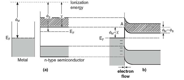
It is essential for further discussion to introduce the work function, f, which is the energy difference between the Fermi energy and the ionization energy. In other words, f is the energy which is necessary to transport an electron from EF to infinity. (Values for f are given in topic 4.)
Let us consider a metal and an n-type semiconductor before they are brought into contact. In Fig. 8.13(a) the Fermi energy of a metal is shown to be lower than the Fermi energy of the semiconductor, i.e., fM > fS. Immediately after the metal and semiconductor have been brought into contact, electrons start to flow from the semiconductor "down" into the metal until the Fermi energies of both solids are equal (Fig. 8.13(b)). As a consequence, the metal will be charged negatively and a potential barrier is formed just as shown in Fig. 8.12. This means that the energy bands in the bulk semiconductor are lowered by the amount![]() with respect to a point A.
with respect to a point A.
Figure 8.13. Energy bands for a metal and an n-type semiconductor (a) before and (b) after contact.![]() The potential barrier is marked with heavy lines. w is the electron affinity.
The potential barrier is marked with heavy lines. w is the electron affinity.
In the equilibrium state, electrons from both sides cross the potential barrier. This electron flow constitutes the so-called diffusion current. The number of electrons diffusing in both directions must be identical for the following reason: the metal contains more free electrons, but these electrons have to climb a higher potential barrier than the electrons in the semiconductor, whose conduction band contains fewer free electrons.
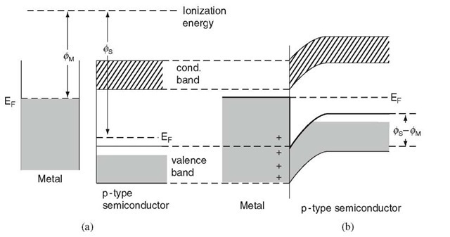
Similarly, if a p-type semiconductor is brought into contact with a metal and f M < f S, then electrons diffuse from the metal into the semiconductor, thus charging the metal and, therefore, the surface of the semiconductor positively. Consequently, a "downward" potential barrier (for the holes) is formed (Fig. 8.14).
In addition to the diffusion current just mentioned, a "drift current" needs to be taken into consideration. Let us assume that an electron-hole pair was thermally created in or near the depletion layer. Then, the thermally created electron in the conduction band is immediately swept down the barrier, and the hole in the valence band is swept up the barrier. This drift current is usually very small (particularly if the band gap is large, such as in GaAs) and is relatively insensitive to the height of the potential barrier. The total current across a junction is the sum of drift and diffusion components.
The potential barrier height for an electron diffusing from the semiconductor into the metal is fM — fS (see Fig. 8.13(b)). This potential difference is called the contact potential. The height of the potential barrier from the metal side is f M — w, where w is the electron affinity, measured from the bottom of the conduction band to the ionization energy (vacuum level) (Fig. 8.13(a)).
Figure 8.14. Energy bands for a metal and a p-type semiconductor (a) before and (b) after contact.![]()
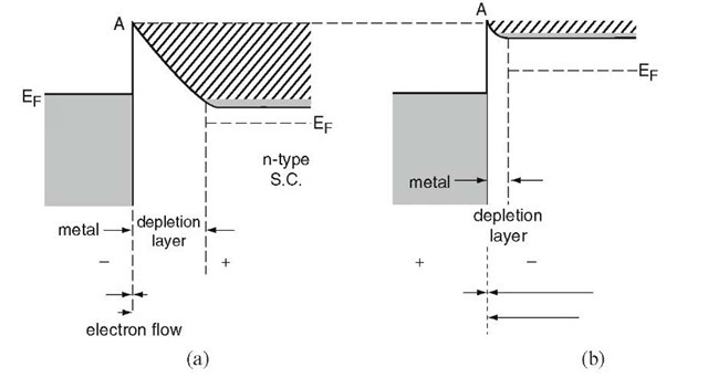
We shall now estimate the net current that flows across the potential barrier when a metal and an n-type semiconductor are connected to a d.c. source (biasing). At first, the metal is assumed to be connected to the negative terminal of a battery. As a result, the metal is charged even more negatively than without bias. Thus, the electrons in the semiconductor are repelled even more, and the potential barrier is increased (Fig. 8.15(a)). Further, the depletion layer becomes wider. Because both barriers are now relatively high, the diffusion currents in both directions are negligible. However, the small and essentially voltage-independent drift current still exists, which results in a very small and constant net electron current from the metal into the semiconductor (reverse bias, Fig. 8.15(a)).
Figure 8.15. Metal-semiconductor contact with two polarities: (a) reverse bias and (b) forward bias. The number of electrons that flow in both directions and the net current is indicated by the length of the arrows. The potential barriers are marked by heavy lines.
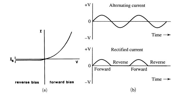
If the polarity of the battery is reversed, the potential barrier in the semiconductor is reduced, i.e., the electrons are "driven" across the barrier so that a large net current from the semiconductor into the metal results (forward bias). The depletion layer is narrow (Fig. 8.15(b)). The voltage-current characteristic of a rectifier is shown in Fig. 8.16(a). Rectifiers of this type are used to convert alternating current into direct current, Fig. 8.16(b).
The current that flows from the metal into the semiconductor is
(see Fig. 8.13b) where A is the area of the contact and C is a constant. The current flowing from the semiconductor into the metal is
where V is the bias voltage (which has the sign of the polarity of the metal) and e is the electronic charge. The net current Inet = ISM — IMS consists of two parts, namely, the saturation current (occasionally called the generation current)13
Figure 8.16. (a) Characteristic of a rectifier. The reverse current is grossly exaggerated! (b) Voltage versus time curves to demonstrate the behavior of an alternating current and a current for which the negative voltage has been eliminated.
and a voltage-dependent term. The net current is then obtained by combining (8.23), and (8.24),
We see from (8.25) that for forward bias (positive V) the net current increases exponentially with voltage. Figure 8.16 reflects this behavior. On the other hand, for reverse bias (negative V) the current is essentially constant and equal to —1S. The saturation current is about three orders of magnitude smaller than the forward current. (It is shown exaggerated in Fig. 8.16.)
We shall learn in Section 8.7.4 that the same rectifying effect as discussed above can also be achieved by using a p-n diode. There are, however, a few advantages in using the metal/semiconductor rectifier. First, the conduction in a metal/semiconductor device involves, naturally, one type of conduction carrier (e.g., electrons) only. Thus, no mutual annihilation of electrons and holes can occur. As a consequence of this lack of "carrier recombination," the device may be switched more quickly from forward to reverse bias and is therefore better suited for microwave-frequency detectors. Second, the metal base provides better heat removal than a mere semiconductor chip, which is helpful in high-power devices.
Ohmic Contacts (Metallizations)
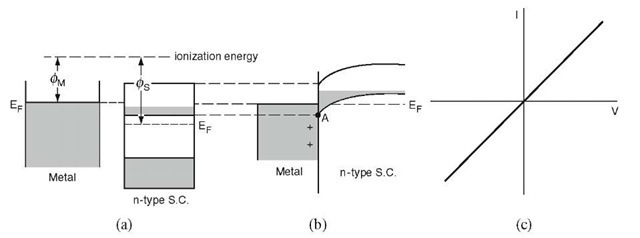
In Fig. 8.17(a) and (b), band diagrams are shown for the case where a metal is brought into contact with an n-type semiconductor. It is assumed that
Figure 8.17. Ohmic contact between metal and n-type semiconductor![]() . (a) Metal and semiconductor are separate. (b) Metal and semiconductor are in contact. (c) Current-voltage characteristic.
. (a) Metal and semiconductor are separate. (b) Metal and semiconductor are in contact. (c) Current-voltage characteristic.
Thus, electrons flow from the metal into the semiconductor, charging the metal positively. The bands of the semiconductor bend "downward" and no barrier exists for the flow of electrons in either direction. In other words, this configuration allows the injection of a current into and out of the semiconductor without suffering a sizable power loss. The current increases, in essence, linearly with increasing voltage and is symmetric about the origin as Ohm’s law requires (Fig. 8.17(c)). Accordingly, this junction is called an ohmic contact. A similar situation exists for a p-type semiconductor and fM > fS.
Aluminum is frequently used for making the contact between a device (e.g., the p-region of a rectifier) and the external leads. Aluminum bonds readily to Si or SiO2 if the device is briefly heated to about 550° C after Al deposition. Since aluminum has a larger work function than silicon (see topic 4) the contact to a p-region is ohmic. Additionally, the diffusion of aluminum into silicon yields a shallow and highly conductive p+-region.14
Now, aluminum is likewise used as a contact material for n-type silicon. To prevent a rectifying contact in this case, one usually lays down a heavily doped and shallow n+-layer14 on top of the n-region. Since this n+-layer is highly conductive and is made to be very thin, tunneling through the barrier accomplishes the unhindered electron flow (see Sections 4.3 and 8.7.8).
p-n Rectifier (Diode)
We learned in Section 8.7.2 that when a metal is brought into contact with an extrinsic semiconductor, a potential barrier may be formed which gives rise to the rectifier action. A similar potential barrier is created when a p-type and an n-type semiconductor are joined.
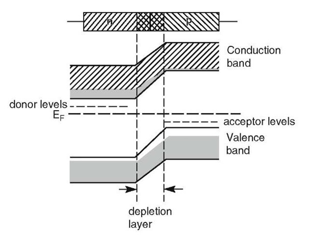
As before, electrons flow from the higher level (n-type) "down" into the p-type semiconductor so that the p-side is negatively charged. This proceeds until equilibrium is reached and both Fermi energies are at the same level. The resulting band diagram is shown in Fig. 8.18.
Consider first the conduction band only. The electrons that want to diffuse from the n-region into the p-region encounter a potential barrier near the junction. For statistical reasons, only a few of them have enough energy to climb the barrier and diffuse into the p-region. The electrons in the p-region, on the other hand, can easily diffuse "down" the potential barrier into the n-region. Note that only a few electrons exist in the conduction band of the p-region. (They have been thermally excited into this band by intrinsic effects.) In the equilibrium state the number of electrons crossing the junction in both directions is therefore identical. (The same is true for the holes in the valence band.)
Figure 8.18. Schematic band diagram for a p-n junction (diode) in equilibrium.
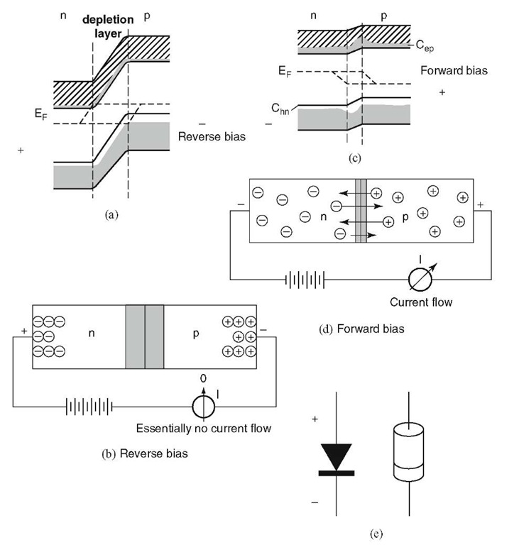
When an external potential is applied to this device, effects similar to the ones described in Section 8.7.2 occur: connecting the positive terminal of a d.c. source to the n-side withdraws electrons and holes from the depletion area which becomes wider and the potential barrier grows higher (Fig. 8.19 (a and b)). As a consequence, only a small drift current (from intrinsic effects) exists (reverse bias). On the other hand, if the n-side is charged negatively, the barrier decreases in height and the space charge region narrows. A large net electron flow occurs from the n-type region to the p-type region (forward bias, Fig. 8.19(c) and (d)).
In Fig. 8.19(a) and (c) "quasi-Fermi levels" for electrons and holes are shown. They are caused by the fact that the electron density varies in the junction from the n-side to the p-side by many orders of magnitude, while the electron current is almost constant. Consequently, the Fermi level must also be almost constant over the depletion layer.
It has to be emphasized that the current in a p-n rectifier is the sum of both electron and hole currents. The net current may be calculated by using an equation similar to (8.25) whereby the saturation current, 1S, in the present case is a function of the equilibrium concentration of the holes in the n-region (Chn), the concentration of electrons in the p-region (Cep), and other device parameters. The saturation current in the case of reverse bias is given by the Shockley equation, which is also called the ideal diode law:
where the D’s and L’s are diffusion constants and diffusion lengths, respectively (e.g., Dep = diffusion constant for electrons in the p-region, etc.). The diffusion constant is connected with the mobility, m, through the Einstein relation:
Figure 8.19. (a) + (b) Reverse and (c) + (d) forward biasing of a p-n junction (diode). (e) Symbol of a p-n rectifier in a circuit and designation of polarity in an actual rectifier. See also Figure 8.16(a).
The minority carrier diffusion length is given by a reinterpretation of a well-known equation of thermodynamics,
where tep is the lifetime of the electrons in the p-type region before these electrons are annihilated by recombination with holes. In order to keep the reverse current small, both Chn and Cep (minority carriers) have to be kept at low levels (compared to electrons and holes introduced by doping). This can be accomplished by selecting semiconductors having a large energy gap (see tables in topic 4) and by high doping.
Zener Diode
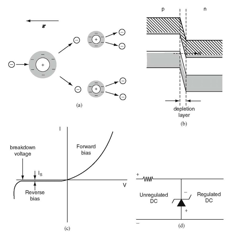
When the reverse voltage of a p-n diode is increased above a critical value, the high electric field strength causes some electrons to become accelerated to a velocity at which impact ionization occurs [Fig. 8.20(a)]. In other words, some electrons are excited by the electric field from the valence band into the conduction band, leaving behind an equal number of holes.
Figure 8.20. (a) Electron avalanche created at breakdown voltage. (b) Tunneling (Zener breakdown). (c) Voltage-current characteristic of a p-n diode exhibiting a breakdown voltage at a large reverse voltage. As in Fig. 8.16(a), Is is shown grossly exaggerated. (d) Zener diode in a circuit for voltage regulation.
The free electrons (and holes) thus created are likewise accelerated and create new electron-hole pairs, etc., until eventually a breakdown occurs, i.e., the reverse current increases quite rapidly (Fig. 8.20(c)). The breakdown voltage, which is the result of this avalanching process, depends on the degree of doping: the higher the doping, the lower the breakdown voltage. Alternatively to this avalanche mechanism, a different breakdown process may take place under certain conditions. It occurs when the doping is heavy and thus the barrier width becomes very thin (i.e., <10 nm). Applying a high enough reverse voltage causes the bands to shift to the degree that some electrons in the valence band of the p-side are opposite to empty states in the conduction band of the n-material. These electrons can then tunnel through the depletion layer, as described in Sections 4.3 and 8.7.8 and depicted in Fig. 8.20(b). Tunneling (or Zener breakdown) takes place usually at low reverse voltages (e.g., below about 4 volts for silicon-based diodes), whereas avalanching is the mechanism that occurs when the reverse voltage is large.
The breakdown effect just described is used in a circuit to hold a given voltage constant at a desired level (Fig. 8.20(d)). The Zener diode is therefore utilized as a circuit protection device. The Zener diode is generally not destroyed by the breakdown, unless excessive heat generation causes it to melt.
![tmp6C412_thumb[2] tmp6C412_thumb[2]](http://what-when-how.com/wp-content/uploads/2011/07/tmp6C412_thumb2_thumb.jpg)
![tmp6C413_thumb[2] tmp6C413_thumb[2]](http://what-when-how.com/wp-content/uploads/2011/07/tmp6C413_thumb2_thumb.jpg)
![tmp6C415_thumb[2] tmp6C415_thumb[2]](http://what-when-how.com/wp-content/uploads/2011/07/tmp6C415_thumb2_thumb.jpg)
![tmp6C416_thumb[2] tmp6C416_thumb[2]](http://what-when-how.com/wp-content/uploads/2011/07/tmp6C416_thumb2_thumb.jpg)
![tmp6C424_thumb[2] tmp6C424_thumb[2]](http://what-when-how.com/wp-content/uploads/2011/07/tmp6C424_thumb2_thumb.jpg)
![tmp6C426_thumb[2] tmp6C426_thumb[2]](http://what-when-how.com/wp-content/uploads/2011/07/tmp6C426_thumb2_thumb.jpg)
![tmp6C427_thumb[2] tmp6C427_thumb[2]](http://what-when-how.com/wp-content/uploads/2011/07/tmp6C427_thumb2_thumb.jpg)
