Introduction
The first observations involving electrical phenomena probably began with the study of static electricity. Thales of Miletus, a Greek philosopher, discovered around 600 BC that a piece of amber, having been rubbed with a piece of cloth, attracted feathers and other light particles. Very appropriately, the word electricity was later coined by incorporating the Greek word elektron, which means amber.
It was apparently not before 2300 years later that man became again interested in electrical phenomena. Stephen Gray found in the early 1700s that some substances conduct electricity whereas others do not. In 1733 DuFay postulated the existence of two types of electricity, which he termed glass electricity and amber electricity dependent on which material was rubbed. From then on a constant stream of well-known scientists contributed to our knowledge of electrical phenomena. Names such as Coulomb, Galvani, Volta, Oersted, Ampere, Ohm, Seebeck, Faraday, Henry, Maxwell, Thomson, and others, come to mind. What started 2600 years ago as a mysterious effect has been applied quite recently in an impressive technology that culminated in large-scale integration of electronic devices.
A satisfactory understanding of electrical phenomena on an atomistic basis was achieved by Drude at the turn of the twentieth century. A few decades later quantum mechanics refined our understanding. Both, the classical as well as the quantum concepts of electrical phenomena will be covered in the topics to come. Special emphasis is placed on the description of important applications.
Survey
One of the principal characteristics of materials is their ability (or lack of ability) to conduct electrical current. Indeed, materials are classified by this property, that is, they are divided into conductors, semiconductors, and nonconductors. (The latter are often called insulators or dielectrics.) The conductivity, s, of different materials at room temperature spans more than 25 orders of magnitude, as depicted in Fig. 7.1. Moreover, if one takes the conductivity of superconductors, measured at low temperatures, into consideration, this span extends to 40 orders of magnitude (using an estimated conductivity for superconductors of about 1020 1/O cm). This is the largest known variation in a physical property and is only comparable to the ratio between the diameter of the universe (about 1026 m) and the radius of an electron (10~14 m).
It is generally accepted that in metals and alloys the electrons, particularly the outer or valence electrons, play an important role in electrical conduction. Therefore, it seems most appropriate to make use of the electron theory that has been developed in the foregoing topics. Before doing so, the reader is reminded of some fundamental equations of physics pertaining to electrical conduction. These laws have been extracted from experimental observations. Ohm’s law,
relates the potential difference, V (in volts), with the electrical resistance, R (in ohms i.e. O), and the electrical current, I (in amps). Another form of Ohm’s law,
links current density,
i.e., the current per unit area (A/cm2), with conductivity, s (I/O cm), and electric field strength,1
Figure 7.1. Room-temperature conductivity of various materials. (Superconductors, having conductivities many orders of magnitude larger than copper, near 0 K, are not shown. The conductivity of semiconductors varies substantially with temperature and purity.) It is customary in engineering to use the centimeter as unit of length rather than the meter. We follow this practice.
(V/cm). (In general, E and j are vectors. For our purpose, however, we need only their moduli.) The current density is frequently expressed by
where N is the number of electrons (per unit volume), v their velocity, and e their charge. The resistance of a conductor can be calculated from its physical dimensions by
where L is the length of the conductor, A is its cross-sectional area, and p is the specific resistance, or resistivity (O cm). We define
The reciprocal of the ohm (O) is defined to be 1 siemens (S); see topic 4.
We discussed in topic 2 the existence of two alternatives to describe an electron. First, we may consider the electrons to have a particle nature. If this model is utilized, one can explain the resistance by means of collisions of the drifting electrons with certain lattice atoms. The more collisions are encountered, the higher is the resistance. This concept qualitatively describes the increase in resistance with an increasing amount of lattice imperfections. It also explains the observed increase in resistance with increasing temperature: the thermal energy causes the lattice atoms to oscillate about their equilibrium positions (see Part V), thus increasing the probability for collisions with the drifting electrons.
Second, one may consider the electrons to have a wave nature. The matter waves may be thought to be scattered by lattice atoms. Scattering is the dissipation of radiation on small particles in all directions. The atoms absorb the energy of an incoming wave and thus become oscillators. These oscillators in turn re-emit the energy in the form of spherical waves. If two or more atoms are involved, the phase relationship between the individual re-emitted waves has to be taken into consideration. A calculation2 shows that for a periodic crystal structure the individual waves in the forward direction are in phase, and thus interfere constructively. As a result, a wave which propagates through an ideal crystal (having periodically arranged atoms) does not suffer any change in intensity or direction. In other words, the electron wave passes without hindrance through an ideal crystal. (Only its velocity is modified.) This mechanism is called coherent scattering.
If, however, the scattering centers are not periodically arranged (impurity atoms, vacancies, grain boundaries, thermal vibration of atoms, etc.) the scattered waves have no set phase relationship and the wave is said to be incoherently scattered. The energy of incoherently scattered waves is smaller in the forward direction, that is, the matter wave loses energy. This energy loss qualitatively explains the resistance. The wave picture provides, therefore, a deeper understanding of the electrical resistance in metals and alloys. In the following two sections we shall calculate the resistance or equivalently, the electrical conduction, using, at first, the particle and then the wave concept.
Conductivity—Classical Electron Theory
Our first approach towards an understanding of electrical conduction is to postulate, as Drude did, a free "electron gas" or "plasma," consisting of the valence electrons of the individual atoms in a crystal. We assume that in a monovalent metal, such as sodium, each atom contributes one electron to this plasma. The number of atoms, Na, per cubic centimeter (and therefore the number of free electrons in a monovalent metal) can be obtained by applying
where N0 is the Avogadro constant, d the density, and M the atomic mass of the element. One calculates about 1022 to 1023 atoms per cubic centimeter,22 23 3 i.e., 10 to 10 free electrons per cm for a monovalent metal.
The electrons move randomly (in all possible directions) so that their individual velocities in the absence of an electric field cancel and no net velocity results. This situation changes when an electric field is applied. The electrons are then accelerated with a force eE towards the anode and a net drift of the electrons results, which can be expressed by a form of Newton’s law (F = ma)
where e is the charge of the electrons and m is their mass. Equation (7.6) implies that as long as an electric field persists, the electrons are constantly accelerated. Equation (7.6) also suggests that after the field has been removed, the electrons keep drifting with constant velocity through the crystal. This is generally not observed, however, except for some materials at very low temperatures (superconductors). The free electron model needs, therefore, an adjustment to take into account the electrical resistance.
An electron, accelerated by an electric field, may be described to increase its drift velocity until it encounters a collision. At this time, the electron has acquired the drift velocity vmax which it may lose, all or in part, at the collision (Fig. 7.2(a)). Alternatively, and more appropriately, one may describe an electron motion to be counteracted by a "friction" force gv which opposes the electrostatic force eE. We postulate that the resistance in metals and alloys is due to interactions of the drifting electrons with some lattice atoms, i.e., essentially with the imperfections in the crystal lattice (such as impurity atoms, vacancies, grain boundaries, dislocations, etc.). Thus, (7.6) is modified as follows:
where g is a constant. The second term in (7.7) is a damping or friction force which contains the drift velocity, v, of the electrons. The electrons are thought to be accelerated until a final drift velocity vf is reached (see Fig. 7.2(b)). At that time the electric field force and the friction force are equal in magnitude. In other words, the electrons are thought to move in a "viscous" medium.
For the steady state case (v = vf) we obtain dv/dt = 0. Then (7.7) reduces to
which yields
Figure 7.2. (a) Schematic representation of an electron path through a conductor (containing vacancies, impurity atoms, and a grain boundary) under the influence of an electric field. This classical model does not completely describe the resistance in materials. (b) Velocity distribution of electrons due to an electrostatic force and a counteracting friction force. The electron eventually reaches the final velocity vf.
We insert (7.9) into (7.7) and obtain the complete equation for the drifting electrons under the influence of an electric field force and a friction force:
The solution to this equation3 is
We note that the factor mvf jeE in (7.11) has the unit of a time. It is customary to define this quantity
as a relaxation time (which can be interpreted as the average time between two consecutive collisions). Rearranging (7.12) yields
We make use of (7.4), which states that the current density, j, is proportional to the velocity of the drifting electrons and proportional to the number of free electrons, Nf (per cm3). This yields, with (7.2),
Combining (7.13) with (7.14) finally provides the sought-for equation for the conductivity,
Equation (7.15) teaches us that the conductivity is large for a large number of free electrons and for a large relaxation time. The latter is proportional to the mean free path between two consecutive collisions. The mean free path is defined to be
Conductivity—Quantum Mechanical Considerations
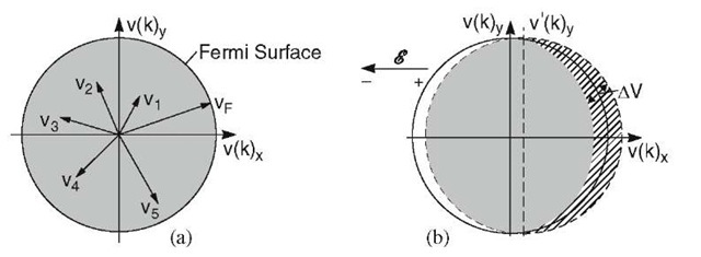
It was stated above that the valence electrons perform, when in equilibrium, random motions with no preferential velocity in any direction. One can visualize this fact conveniently by plotting the velocities of the electrons in velocity space (Fig. 7.3(a)). The points inside a sphere (or inside a circle when considering two dimensions) correspond to the endpoints of velocity vectors. The maximum velocity that the electrons are able to assume at T = 0 is the Fermi velocity, vF (i.e., the velocity of the electrons at the Fermi energy). The sphere having vF as a radius represents, therefore, the Fermi surface. All points inside the Fermi sphere are occupied. As a consequence the velocity vectors cancel each other pairwise at equilibrium and no net velocity of the electrons results.
If an electric field is applied, the Fermi sphere is displaced opposite to the field direction, i.e., towards the positive end of the electric field, due to the net velocity gain of the electrons (Fig. 7.3(b) dashed circle). The great majority of the electron velocities still cancel each other pairwise (shaded area). However, some electrons remain uncompensated; their velocities are shown cross hatched in Fig. 7.3(b). These electrons cause the observed current. The Drude description of conduction thus needs a modification. In the classical picture one would assume that all electrons drift, under the influence of an electric field, with a modest velocity. Quantum mechanics, instead, teaches us that only specific electrons participate in conduction and that these electrons drift with a high velocity which is approximately the Fermi velocity vF.
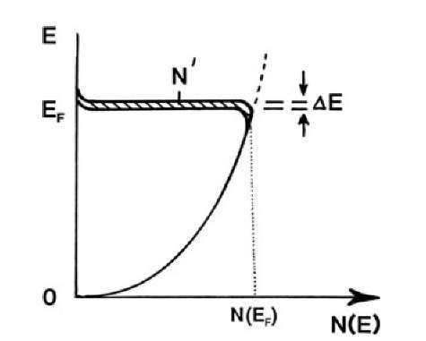
An additional point needs to be discussed and leads to an even deeper understanding. The largest energy which the electrons can assume in a metal at T = 0 is the Fermi energy EF (topic 6). A large number of electrons actually possess this very energy since the density of states and thus the population density is highest around EF (Fig. 7.4). Thus, only a little extra energy DE is needed to raise a substantial number of electrons from the Fermi level into slightly higher states. As a consequence, the energy (or the velocity) of electrons accelerated by the electric field E is only slightly larger than the Fermi energy EF (or the Fermi velocity vF) so that for all practical purposes the mean velocity can be approximated by the Fermi velocity, vF. We implied this fact already in our previous discussions.
Figure 7.3. Velocity of electrons in two-dimensional velocity space. (a) Equilibrium and (b) when an electric field is applied. The shaded areas to the left and right of the v(k)y-axis are of equal size. They cancel each other. The cross-hatched area remains uncompensated.
Figure 7.4. Population density N(E) versus energy for free electrons (see Fig. 6.5) and displacement DE by an electric field (see Fig. 7.3(b)). N is the number of displaced electrons per unit volume (see (6.11a)) in the energy interval DE. N(E) is defined per unit energy and, in the present case, also per unit volume, see (6.8).
We now calculate the conductivity by quantum mechanical means and apply, as before, Ohm’s law j = oE, (7.2). The current density j is, as stated in (7.4), the product of the number of electrons, the electron velocity, and the electron charge. In our present case, we know that the velocity of the electrons which are responsible for the electron conduction is essentially the Fermi velocity, vF. Further, the number of electrons which need to be considered here is N0, i.e., the number of displaced electrons per unit volume, as shown in Fig. 7.4. Thus, (7.4) needs to be modified to read
The number of electrons displaced by the electric field E is
(see Fig. 7.4), which yields for the current density
The factor dE/dk is calculated by using the E versus Ikl relationship known for free electrons (4.8), i.e.,
Taking the first derivative of (7.19) yields, with
Inserting (7.20) into (7.18) yields
The displacement, Dk, of the Fermi sphere in k-space under the influence of an electric field can be calculated by using (7.6) and p = hk (4.7):
which yields
or
where t is the time interval Dt between two "collisions" or the relaxation time (see Section 7.3). Inserting (7.23) into (7.21) yields
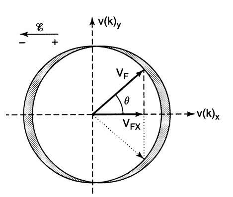
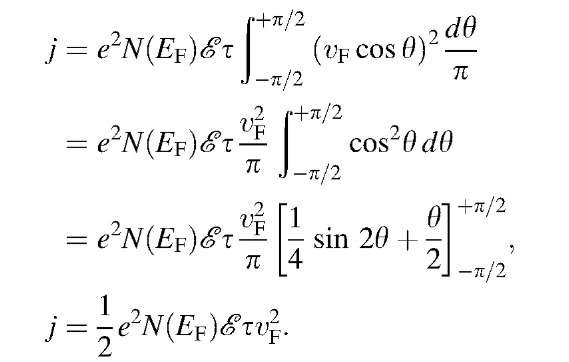
One more consideration needs to be made. If the electric field vector points in the negative v(k)x direction, then only the components of those velocities that are parallel to the positive v(k)x direction contribute to the electric current (Fig. 7.5). The v(k)y components cancel each other pairwise. In other words, only the projections of the velocities vF on the positive v(k)x-axis (vFx = vF cos 9) contribute to the current. Thus, we have to sum up all contributions of the velocities in the first and fourth quadrants in Fig. 7.5, which yields
Figure 7.5. Two-dimensional velocity space.
A similar calculation for a spherical Fermi surface yields
Thus, the conductivity finally becomes, with
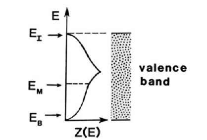
This quantum mechanical equation reveals that the conductivity depends on the Fermi velocity, the relaxation time, and the population density (per unit volume). The latter is, as we know, proportional to the density of states. Equation (7.26) is more meaningful than the expression derived from the classical electron theory (7.15). Specifically, (7.26) contains the information that not all free electrons Nf are responsible for conduction, i.e., the conductivity in metals depends to a large extent on the population density of the electrons near the Fermi surface. For example, monovalent metals (such as copper, silver, or gold) have partially filled valence bands, as shown in Figs. 5.22 or 6.7. Their electron population densities near their Fermi energy are high (Fig. 7.6), which results in a large conductivity according to (7.26).
Figure 7.6. Schematic representation of the density of states (Fig. 6.6) and thus, with minor modifications, also the population density (6.7). Examples for highest electron energies for a monovalent metal (EM), for a bivalent metal (EB), and for an insulator (EI) are indicated.
Bivalent metals, on the other hand, are distinguished by an overlapping of the upper bands and by a small electron concentration near the bottom of the valence band, as shown in Fig. 6.7(c). As a consequence, the electron population near the Fermi energy is small (Fig. 7.6), which leads to a comparatively low conductivity. Finally, insulators and semiconductors have, under certain conditions, completely filled electron bands, which results in a virtually zero population density near the top of the valence band (Fig. 7.6). Thus, the conductivity in these materials is extremely small.


