Laser Amplifier
The laser can also function as an optical amplifier, which is again used for telecommunication purposes. A weak optical signal enters a laser through one of its windows and there stimulates the emission of photons.
The amplified signal leaves the other window after having passed the cavity only once. This traveling-wave laser is biased slightly below the threshold current in order to exclude spurious lasing not triggered by an incoming signal. Nevertheless, some photons are always spontaneously generated, which causes some background noise.
A new development is the erbium-doped fiber amplifier, which works quite similar to the above-mentioned traveling-wave laser. Erbium atoms, contained in lengths of a coiled glass fiber, are pumped to higher energies by an indium-gallium- arsenide-phosphide laser at a wavelength of 0.98 mm or 1.48 mm. When a weakened signal enters one end of this erbium-doped fiber, the erbium atoms gradually transfer their energy to the incoming signal by stimulated emission, thus causing amplification. A mere 10 mW of laser power can thus achieve a gain of 30-40 dB. Networks which include fiber amplifiers, linked at certain distance intervals to cladded optical glass fibers (Fig. 13.30), have the potential of transmitting data at very high rates, e.g., 2.5 gigabits of information per second over more than 20,000 km. This is possible because fibers are able to support a large (but finite) number of channels. The advantage of erbium-doped optical fibers is that they do not interrupt the path of a light signal as conventional "repeaters" do (which convert light into an electric current, amplify the current, and then transform the electrical signal back into light).
Quantum Well Lasers
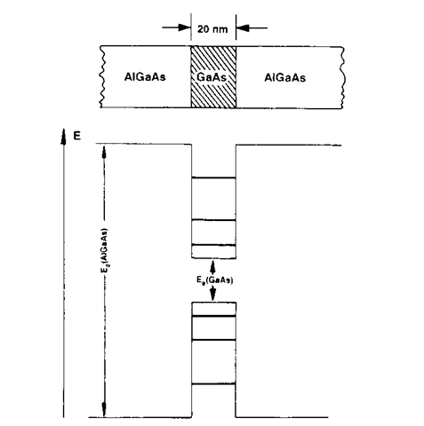
Quantum well lasers are the ultimate in miniaturization, as already discussed in Section 8.7.10. We have explained there that some unique properties are observed when device dimensions become comparable to the wavelength of electrons. In essence, when a thin (20 nm wide) layer of a small-band gap material (such as GaAs) is sandwiched between two large-band gap materials (such as AlGaAs), a similar energy configuration is encountered as known for an electron in a box (Fig. 8.33). Specifically, the carriers are confined in this case to a potential well having "infinitely" high walls. Then, as we know from Section 4.2, the formerly continuous conduction or valence bands reduce to discrete energy levels, see Fig. 13.45.
The light emission in a quantum well laser occurs as a result of electron transitions from these conduction band levels into valence levels. It goes almost without saying that the line width of the emitted light is small in this case, because the transitions occur between narrow energy levels. Further, the threshold current density for lasing (Fig. 13.41) is reduced by one order of magnitude, and the number of carriers needed for population inversion is likewise smaller.
If a series of large-and small-band gap materials are joined, thus forming a multiple quantum well laser, the gain is even further increased and the stability of the threshold current toward temperature fluctuations is improved.
Figure 13.45. Band structure of a single quantum dot structure.
The GaAs/GaAlAs combination yields an emission wavelength somewhat below 0.87 mm, whereas InGaAsP quantum well lasers emit light near 1.3 mm or 1.5 mm (depending on their composition). It appears to be challenging to eventually fabricate quantum wire or quantum dot lasers (see Section 8.7.10) which are predicted to have even lower threshold current densities and higher modulation speeds.
Light-Emitting Diodes (LED)
Light-emitting diodes are of great technical importance as inexpensive, rugged, small, and efficient light sources. The LED consists, like the semiconductor laser, of a forward biased p-n junction. The above mentioned special facing procedures are, however, omitted during the manufacturing process. Thus, the LED does not operate in the lasing mode. The emitted light is therefore neither phase coherent nor collimated. It is, of course, desirable that the light emission occurs in the visible spectrum. Certain III-V compound semiconductors, such as GaxAs1_xP, GaP, GaxAl1_xAs (for red and yellow-green) and the newly discovered nitride-based compound semiconductors (for green and blue colors) fulfill this requirement. Their emission efficiencies (measured in lumens per watt) are at par or even better than those of unfiltered incandescent light bulbs and are almost one order of magnitude larger than certain color-filtered tungsten-filament lamps. All three basic colors necessary for covering the visible spectrum and also the infrared (450-1,500 nm) are now available with adequate intensities. Because of these properties, the lighting industry is currently undergoing a revolution that will lead to LED-based large flat-panel color displays, bright outdoor color signs, better projection television, full-color photographic printers, more efficient and particularly durable traffic lights, and even changes in home and office illumination.
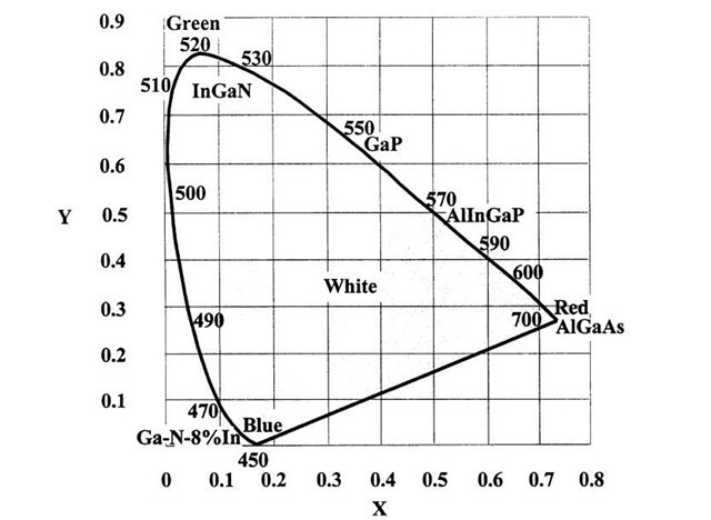
In order to vividly demonstrate the spectral emission properties of LEDs a chromaticity diagram as shown in Fig. 13.46 is helpful. It is based on the peculiarities of the three types of cones in the human eye, which are sensitive for either blue, green, or red radiation. (The corresponding wavelengths mark the corners of the chromaticity diagram). A given "color" is represented by two parameters or percentages (x and y) in this graph, while the percentage of the third color is the difference between x + y and 100%. Monochromatic light (such as from a laser) is depicted by a specific point on the perimeter of the graph. Any other hue is created by mixing the basic colors. When the spectral width of the light increases and the emission is therefore less pure, the color coordinates move towards the center. As an example, "white light", that is, the broad emission spectrum of a black-body radiator heated to very high temperatures (e.g., the sun), is described by a point in this diagram at which x as well as y are about 33%.
Figure 13.46. Chromaticity diagram in which the positions of some commercially available LEDs are shown.
Figure 13.46 displays the color coordinates of some of the presently available electroluminescing compound semiconductors. Ga-N containing about 8% In is depicted to provide blue (470 nm) light. This color changes into green (520 nm) by adding successively larger amounts of indium to GaN. Al-Ga-As yields red hues (700 nm) and yellow-green light is emitted by Al-In-Ga-P (590 nm). Moreover, green- or blue-emitting LEDs, when covered by one or more appropriate phosphors, (see Section 13.8.1) can be made to vary their color according to the spectral emission of the phosphor. White-radiating LEDs are obtained by exciting suitable phosphors by the ultraviolet radiation from GaN. Alternatively, white-emitting LEDs are obtained by adding blue and yellow LED light.
A few technical details on nitride-based semiconductors shall be added. As mentioned above, LEDs require n-and p-type components to manufacture a diode. Si in the form of silane (SiH4) is used for n-doping. On the other hand, incorporating Mg, followed by low-energy electron radiation, or thermal annealing (to activate the Mg-doped GaN) leads to p-type segments.
As already mentioned in Section 13.8.9 (Fig. 13.43), double hetero-structures increase the output power of LEDs. Specifically, incorporating Zn and Si dopants into an In-Ga-N active layer that is surrounded by Al-Ga-N layers leads to output powers near 3 mW when the chip size is 3 x 3 mm2. Further, a peak wavelength of 450 nm, and an external quantum efficiency of 5.4% (that is, the ratio of the number of photons produced to the number of injected electrons) are obtained. Forward currents of typically 20 mA are generally applied.
The devices consisting of indium-gallium nitrides are commonly deposited on sapphire (a-Al2O3) or silicon carbide (6H-SiC) substrates. Metal-organic chemical vapor deposition at 700 to 1,100°C, involving trimethyl gallium (Ga(CH3)3) and ammonia (NH3) as gas sources, is generally used for growing epitaxial GaN films. InGaN is laid down by additions of trimethyl indium. The devices are contacted and eventually encapsulated in epoxy resins. The radiation leaves the device through a semitransparent metal contact on the top or through a transparent n-GaN contact on the substrate. In the case of GaAs, the light may leave the device through a window which has been etched through the metallic contact (surface emitter).
The "lifetimes" of LEDs are extrapolated to be in excess of 50,000 hours, or more precisely, the time after which the light intensity has decreased to 70% of its original value is approximately 30,000 hours. (This compares to an average lifetime of 1,000 to 2,000 hours for a typical incandescent light bulb.) The failures are generally caused by a break-down of the contacts or the encapsulate, rather than of the semiconductor itself. The cost at present is about one US dollar for a blue- or green-emitting diode and less than 10 cents for red and orange LEDs.
A short note on other recently developed LED materials shall be added. Blue-emitting SiC has been investigated for some time, but its efficiency is orders of magnitude smaller than the above-described nitrides. This is mainly due to its indirect-band gap characteristics. ZnSe (a II-VI compound) has also blue and green emissions, but its lifetime is substantially reduced by the formation of structural defects. LEDs based on polymers with ionic materials as electron-injecting and hole-blocking layers have been demonstrated. Finally, as a matter of curiosity, a "light-emitting vegetable diode", utilizing a pickle, has been reported in the literature to emit yellow light (and an unpleasant smell).
Organic Light Emitting Diodes (OLEDs)
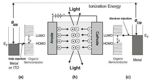
Organic light emitting diodes work in principal quite similar to inorganic LEDs like gallium-arsenide-phosphide (or GaN) diodes as described in the previous section. Specifically, electrons and holes are injected from opposite sides (called cathode and anode, respectively) into a suitable organic material where they combine to form electron/hole pairs (called excitons, see Section 13.6) and then relax to the ground state by emitting photons. This is shown schematically in Fig. 13.47(b). In order to obtain a high rate of hole injection, and thus, a good light emitting efficiency, it is important to match the work function of the anode (e.g. metal) electrode, 0AM, that is, the Fermi energy, EF, (Fig. 8.13) with the HOMO level (Section 9.1) of the organic semiconductor.
Figure 13.47. Schematic representation of a single-layer organic light emitting diode. (a) A metal "band diagram" adjacent to HOMO/LUMO levels of an organic semiconductor is depicted. Hole injection is indicated. (b) Schematic functioning of a single layer OLED. (c) HOMO/LUMO levels and metal "band diagram" for electron injection.
This is schematically depicted in Fig. 13.47(a). Likewise, a high efficiency of electron injection is achieved by matching the LUMO level of the organic semiconductor with the work function of the metal cathode, 0CM; see Fig. 13.47(c). The match between HOMO levels and metals is generally easily achieved because of the high work function of many metals; see the tables in topic 4. Likewise, many metal oxides, such as transparent Indium-Tin-Oxide (ITO) or GaInO3 or ZnInSnO, (see Section 9.3), have large work functions which are close to the HOMO level of some organic semiconductors, such as diamine (Fig. 13.48(a)), and are therefore used for anodes. On the other hand, metals which have the required low work function, 0CM, to match with the LUMO level (Fig. 13.47(c)) are often highly reactive and susceptible to corrosion under the influence of moisture and oxygen.
A further point needs to be considered: Even if the number of injected electrons and holes are the same, the mobilities of these carriers may still be different (topic 4). This may lead to non-radiative recombination of holes and electrons (near the interface between metals and organic semiconductors) and as a consequence, to a low light emitting efficiency and a high driving voltage. Other device structures are therefore necessary, as described momentarily.
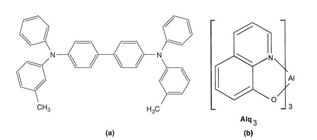
An improvement is obtained by a double-layer OLED which consists, for example, of a transparent ITO coating on a glass substrate as an anode, a diamine film for hole transport, tris(8-hydroxyquinoline) aluminum (Alq3) as an electron transporting and light emitting layer, and finally a magnesium-silver alloy as a cathode, see Figures 13.48 and 13.49. As mentioned above, the work function of ITO matches the HOMO level of the diamine which leads to an efficient hole injection.
Figure 13.48. Chemical compounds for OLEDs. (a) N,N’,-diphenyl-N,N’-bis(3-methylphe-nyl)-(1,1′-biphenyl)-4,4′-diamine (TPD) (b) Alq3 also known as tris(8-hydroxyquinoline) aluminum having the formula Al(C9H6NO)3.
Figure 13.49. Double-layer organic light emitting diode.
On the other hand, the work function of the (non-corrosive) magnesium-silver alloy is close to the LUMO level of Alq3. This array increases the rate of carrier injections, the carrier mobilities, and the device efficiency. Moreover, the operating voltage may be reduced to below 10 V due to the total layer thickness of about 200 nm. Since diamine provides a higher hole mobility compared to the electron mobility in Alq3, while Alq3 provides a reasonably high electron mobility, the exciton formation takes place close to the diamine/Alq3 interface to yield green light. Other colors can be achieved by varying the band gap of the emitter material.
The efficiency of an OLED can be further improved by utilizing multilayer devices. The principle of their built-up is quite similar to that shown in Figure 13.47, consisting of anode (hole injection layer), hole transport layer, light emitting zone, electron transport /electron injection layer, and cathode. By proper materials selection, it is possible to design a device so that the electron transport layer provides a high electron mobility (and the hole transport layer provides a high hole mobility). Moreover, it is desirable that one type of carrier is blocked in the transport layer of the opposite polarity. For example, electrons should be allowed to freely diffuse in the electron transport layer while the holes should be blocked there. This can be accomplished by proper band-gap engineering and materials selection.
Finally, OLEDs may be arranged in stacks which are electrically connected in series. Each of the individual OLEDs can be made to emit a different color which allows white emission. The individual units of these tandem devices operate at lower current densities and reduced voltages. (High current densities and operating voltages cause premature degradation and lead to lower quantum efficiencies).
A few words should be added about the advantages (and disadvantages) of OLEDs. Most of all, the technology for processing organics (for example synthesizing and depositing on a substrate) is much less demanding compared to inorganic LEDs. Specifically, polymers are frequently deposited from a solution, such as by spin-coating from a solution, direct printing by contact with stamps, or by ink-jet printing. Small molecules are vapor deposited in vacuum, as is common for metals. This allows an easy tailoring of properties of OLEDs to specific demands (color, driving voltage, lifetime, etc.) as described above. Moreover, organic materials can be produced in the form of films which make them flexible. On the other hand, the primary problems of OLEDs are stability issues, specifically, degradation due to high current densities, and corrosion of some electrode metals under the influence of moisture and oxygen. Still, lifetimes (50% reduction of original intensity) of up to 100,000 hours for red emitters (and even extrapolated lifetimes of 300,000 to 500,000 hours for red and green emitters) have been reported. Considerable research in this field with the goal of producing inexpensive displays and lighting is presently being conducted. Indeed, OLED displays are already available in various consumer products such as mobile phones, MP3 players, digital cameras, auto radios, etc. Thus, the improvements and further developments of OLEDs should be followed with considerable anticipation.


