Biomedical Engineering Reference
In-Depth Information
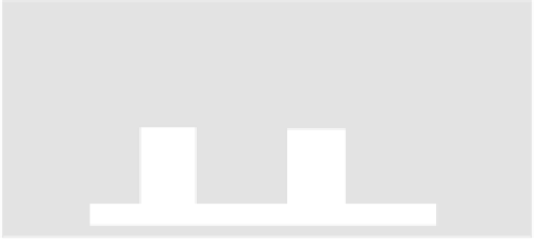
40 nm
InAs
InP
5nm
0.6 eV
15 nm
E
c
Fig. 1.28
Circular nanowire InP/InAs superlattice (
top
) and its conduction band diagram (
bottom
)
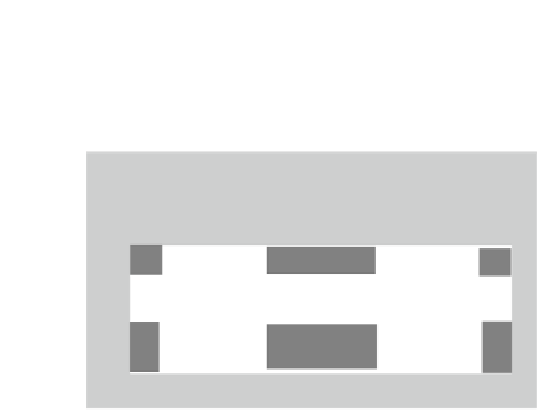
Fig. 1.29
Carbon nanotube
superlattice (
top
) and its
energy band diagram
(
bottom
)
H
2
Intrinsic CNT
E
c
1 eV
E
g
0.6 eV
2 eV
E
v
hydrogen functionalized semiconducting CNT; the energy bandgaps E
g
of these
material differ (
Gulseren et al. 2003
).
Both superlattices display a marked negative differential resistance and, as
resonant tunneling diodes, can generate electromagnetic radiation with very high
frequencies or can be employed as logic elements. The nanowire superlattice can
be seen also as a series of three-dimensionally confined quantum dots, the transport
through the structure taking place via coherent tunneling between adjacent quantum
dots. If the width of the quantum barrier region increases, the tunneling process
becomes sequential.
As in the case of core/shell nanoparticles, nanowire superlattices with radial
periodicity can be fabricated by growing several nanowire shells with dissimilar
properties. Typical examples are the coaxial Ge/Si and Si/Ge nanowires, obtained
by initially growing one nanowire using the VLS method and then applying
CVD deposition methods to grow the second nanowire over the first one (
Lauhon
et al. 2002
).
Besides growing nanowires with prescribed properties, it is also important to
align and position them using self-assembly techniques. Millions of CNTs, for
example, can be aligned via a large-scale assembly method similar to biomolecular
self-assembly processes (
Rao et al. 2003
). In this technique, millions of CNTs
spread in solution are aligned on top of chemically functionalized patterns fabricated
on a surface. The functionalization is achieved with two distinct regions, which are


Search WWH ::

Custom Search