Biomedical Engineering Reference
In-Depth Information
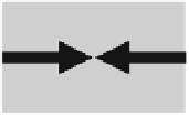
Fig. 9.7
(
a
) Arrow-shaped
drain (D) and source (S)
electrodes in a biological
transistor and (
b
) a typical
current-voltage characteristic
a
b
I
S
D
substrate
V
molecule is placed over the central part of the CNT, on which a 50-nm-wide channel
is fabricated with the focused ion-beam bombardment technique. The poly(dG)-
(dC) DNA molecule, placed using the electromagnetic trapping method, increases
the electrical conductivity between CNT electrodes, acting as a p-type channel. The
room-temperature current-voltage characteristic, which has a typical form as that
in Fig.
9.6
b, can be explained by the small polaron hopping model, the hopping
transport mechanism being different for low- and high-bias voltage ranges. More
specifically, the estimated hopping distance is 9.08 A for biases between
10 and
10 V; this parameter decreases to 3.8 A if the whole
20-20 V bias range is taken
into consideration. The latest value is comparable to the 3.4 A distance between base
pairs in the DNA molecule. Metallized DNA, consisting of arrays of Co
2C
; Zn
2C
,
or Ni
2C
metal ions that substitute the imino protons of every base pair, can also be
used as the active element of a FET, the rate of the phonon-assisted electron hopping
between the localized states of metal ions being strongly influenced by a transverse
electric field (
Nokhrin et al. 2007
).
Electrical transport between nanosized Cr/Au arrow-shaped source and drain
electrodes bridged by self-assembled guanosine ribbons and placed above a back
gate Ag electrode has been demonstrated in
Maruccio et al.
(
2003
). This FET,
shown in Fig.
9.7
, has a p-type channel consisting of ribbon-shaped supramolecular
assembles of deoxyguanosine derivatives that induce current rectification due to the
intrinsic dipole moment oriented along the ribbon axis, which creates a preferential
charge pathway. When the currents I are measured for both polarizations of
the source-drain voltage V , the rectification ratio is found to be RR.V/
D
I.V/=I.
V/
Š
3. In fact, the current increases slowly, almost linearly with the
source-drain voltage up to about 3 V, and shows an exponential increase above this
threshold voltage, which depends slightly on the gate bias. In fact, although similar
to a MOSFET, this biomolecular FET differs from the latter in that the current-gate
voltage dependence does not saturate for a given source-drain voltage, indicating
the presence of two transport mechanisms: energy band alignment and resonant
transport in the molecular channel.
Biological organic FETs have been fabricated also from DNA-based polymers
such as insulating DNA-CTMA thin films, but these devices often show large
hysteresis caused by ionic charge migration, which limits their performances. In
addition, DNA-CTMA films are soft and can be easily scratched. A significant
improvement of both electrical and mechanical properties of DNA-CTMA
FETs containing DNA purified from salmon waste occurs after cross-linking
with
poly(phenylisocyanate)-
co
-formaldehyde (PPIF)
(
Yumusak
et
al.
2009
).

Search WWH ::

Custom Search