Environmental Engineering Reference
In-Depth Information
that P-MOS Q1, and in turn N-MOS Q2, remain on when the voltage across
C2 drops below the Zener diode's breakdown voltage. This is because once
the source and load ground are connected, current flows through R3, thus
maintaining a voltage at the gate of P-MOS Q1 to latch the regulator to the
capacitor. The capacitor C2 stops discharging once the voltage across it falls
to an extent that the voltage across R2 is below the threshold voltage of Q2.
The duration of the discharge must be at least as long as the time required
to transmit three successive RF signals, so that the RF receiver can acknowl-
edge the transmission and turn on/off the electronic appliance to which it is
attached.
4.2.4
Experimental Results
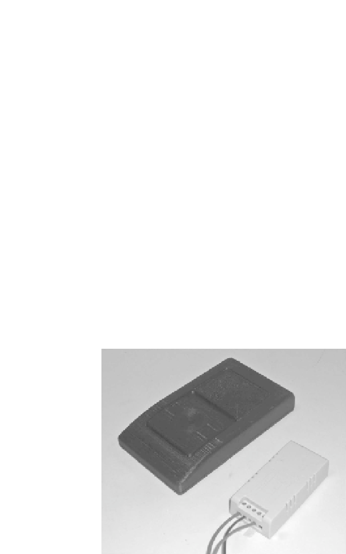
To demonstrate the feasibility of this proposed impact-based energy harvest-
ing system using a prestressed piezoelectric diaphragm material, the hard-
ware prototype of the batteryless wireless control switch has been imple-
mented [121] as shown in
Figure 4.23
.
The component values of the schematic diagram of the proposed impact-
based energy harvesting system shown in
Figure 4.22
are determined with the
following considerations: The first component to decide is capacitor C2. As
analyzed previously, 10
F was chosen as it has a peak voltage of about 12 V;
it also has a suitable discharge time constant and stores sufficient energy for
wireless transmission (
0.836 mJ). A complementary MOSFET (N-MOS and
P-MOS) is chosen as it has a low threshold voltage (1.0 V) and is conveniently
placed together as a single component. Therefore, a Zener diode with a reverse
∼
Self-Powered
Wireless RF
Transmitter
RF Receiver to Switch the
Electrical Appliance On/Off
FIGURE 4.23
Prototype of a proposed batteryless wireless control switch using prestressed piezoelectric
diaphragm material.


Search WWH ::

Custom Search