Biomedical Engineering Reference
In-Depth Information
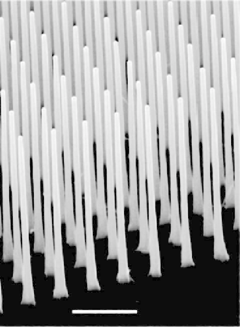
FIGURE 12.9
SEM of InP nanowires grown with MOVPE
from gold catalysts defined by electron
beam lithography. (From Samuelson, L.,
Thelander, C., Bjork, M. T., Borgstrom, M.,
Deppert, K., Dick, K.A., Hansen, A. E.,
Martensson, T., Panev, N., Persson, A. I.,
Seifert, W., Skold, N., Larsson, M. W.,
Wallenberg, L. R. (2004). Semiconductor
Nanowires for 0D and 1D Physics and
Application.
Physica E.
, 25, 313-318.)
1
µ
m
12.3.2
Synthesis of Nanowires
Synthesis methods of NWs include both vapor phase and solution techniques. Compared
with physical methods such as nanolithography and other patterning techniques,
chemical methods are seen to be more versatile and effective in the synthesis of these
NWs. The chemical synthesis includes various routes: thermal evaporation, chemical
vapor-phase deposition, metal-organic chemical vapor-phase deposition, arc discharge,
laser ablation, sol-gel, and template-based methods. The basic process of 1D nanostruc-
ture formation involves two fundamental steps: nucleation and growth. A major chal-
lenge in the synthesis of NWs is to control their size, phase purity, crystallinity, and
chemical composition. Therefore, a detailed understanding and good control of the
nucleation and growth processes at the nanometer scale is required.
12.3.2.1
Vapor Phase Growth of Nanowires
12.3.2.1.1 Vapor-Liquid-Solid Growth
The vapor-liquid-solid (VLS) mechanism was proposed by Wagner [52] in the 1960s,
when he studied the growth of millimeter-scale Si whiskers using Au as catalyst. An
advantage of the VLS method is that it can produce single-crystalline 1D nanostructures
from a rich variety of inorganic materials including elemental semiconductors (Si, Ge, and
B), III-V semiconductings (GaN, GaAs, GaP, InP, and InAs), II-VI semiconductors (ZnS,
ZnSe, CdS, and CdSe), and oxides (ZnO, MgO, and SiO
2
) [47]. A typical VLS process
involves the dissolution of gaseous reactants into nanosized liquid droplets of a catalyst