Biomedical Engineering Reference
In-Depth Information
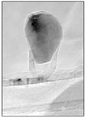
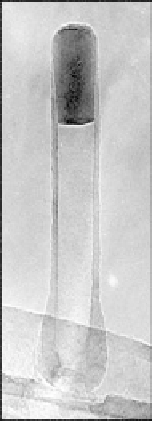
FIGURE 12.8
TEM micrographs of the initiation
of MWCNT growth. (A) A cat-
alytic particle before the growth
of a nanotube. (B) The graphene
layers initiate from the bottom of
the catalyst at an inclination with
respect to the tube. (C) The cat-
alytic particle is lifted up from the
substrate as the tube forms. (D)
The length of the tube increases
and the catalytic particle becomes
cork-shaped. (Reproduced with
permission from Sun, X., Li, R.,
Stansfield, B., Dodelet, J. P.,
Ménaed, G., Désilets, S. (2006).
Controlled Synthesis of Pointed
Carbon Nanotubes.
Carbon
, in
press.)
25 nm
45 nm
(A)
30 nm
30 nm
(B)
(C)
(D)
bottom. These spherical graphitic layers at the bottom (Figure 12.8D) correspond to the
shape of the catalytic particle at the initial stage. Subsequently, the bottom of the catalyst
particle separates from the lateral graphitic layers. The catalyst is then lifted up, maintain-
ing a facet at the bottom while becoming round at the top (Figure 12.8C). Continued growth
leads to a cork-shape catalyst with uniform walls (Figure 12.8D).
In conclusion, different structures may depend on different synthesis methods.
Compared with the nested concentric structure of MWCNTs, scrolled structures appear to
have many advantages. The high reactivity of the edges of the graphene sheet facilitates
surface functionalization by, for example, -OH, -COOH, or deposition of other metals
such as Pt, which is useful for various applications such as biosensors.
12.3
Nanowires
12.3.1
Introduction
Nanowires (NWs), like CNTs, are also 1D and well-defined crystalline structures with a
high aspect ratio. NWs have been demonstrated to possess superior electrical, optical,
mechanical, and thermal properties. Unlike CNTs, NWs are noncarbon-based materials
that can consist of metals, semiconductors, or inorganic compounds. The broader choice
of various crystalline materials and doping methods makes the electronic and optical
properties of NWs tunable with a high degree of freedom and precision. With the devel-
opment of new synthesis methods, NWs have attracted increasing attention for sensor
applications.
Nature
magazine recently stated that “Nanowires, nanorods, nanowhiskers,
it does not matter what you call them, they are the hottest properties in nanotechnology”
(
Nature
, 419 (2002) 553). Figure 12.9 shows a well-aligned array of InP NWs grown from
gold catalyst particles defined by electron beam lithography [45]. There are a few reviews
[46,47] and topics [48-51] dealing with the synthesis, characterization, properties, and
applications of these materials. A grand challenge is to integrate NWs into assemblies with
multifunctions to fabricate nanoscale electronic and photonic devices as well as biosen-
sors. In this section, we will focus on their synthesis, growth process, and properties.