Biomedical Engineering Reference
In-Depth Information
either interband absorption or free-carrier absorption. It might, therefore, be
possible to obtain less than 1.0 dB cm
−1
loss over the entire wavelength range
of 0.82-1.3 μm; however it is very difficult to couple light from a device such
as a laser or modulator in the GaAs wafer into the waveguide without con-
siderable coupling loss because the index of refraction of GaAs is so much
larger than that of the dielectric. The three exposed surfaces of the dielec-
tric waveguide are also subject to damage and degradation due to physical
abrasion and atmospheric contaminants. To act as a waveguiding region the
deposited film would need to be isolated from the GaAs substrate by another
film having a lower refractive index than the waveguiding film. In the past
it has been difficult to deposit such a two-layer structure and achieve low
waveguiding loss. There is also the possibility of the waveguide lifting from
the GaAs surface because of mismatch in the thermal expansion coefficients.
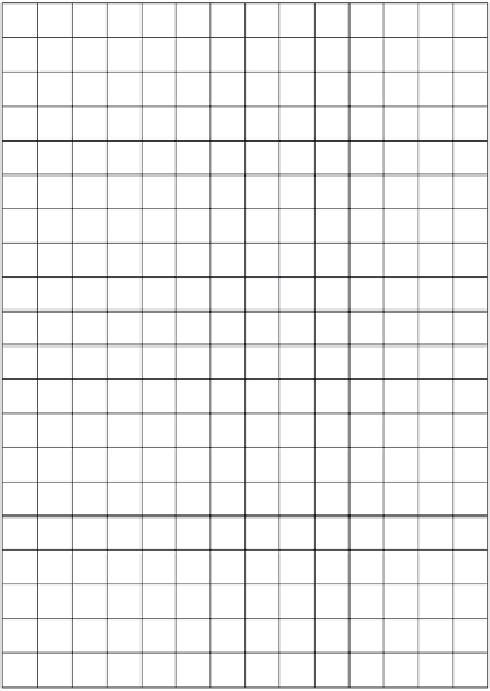
20
19
18
17
16
15
Kuznetsov
14
13
12
Marcatili
11
10
9
8
7
λ
0
= 10.6 µm
a
=
b
= 9.0 µm
N
D
= 5 ×10
17
cm
-3
α= 2.45 dB cm
-1
6
5
4
Parallel channel
directional coupler
L
versus
C
3
2
1
0
1
2
3
4
5
6
7
8
9
10
11
12
13
14
(d)
C
(µm)
FIGURE 5.14 (continued)
(d) λ
0
= 10.6 μm;
a = b
= 9.0 μm;
N
D
= 5 × 10
17
cm
−3
; α = 2.45 db cm
−1
parallel direction channel direc-
tional coupler
L
versus
C
.
(
continued
)

Search WWH ::

Custom Search