Biomedical Engineering Reference
In-Depth Information
Hydrogen was implanted into the polished silicon wafers using PIII in the plasma laboratory of
the City University of Hong Kong. The chamber was evacuated to 0.6 Torr, and high-purity hydrogen
gas was bled into the vacuum chamber to establish a working pressure of 0.5 mTorr. The instru-
mental parameters are listed in Table 19.1. Under these conditions, H
+
is the dominant ion species in
the plasma [48]. Unlike beam-line ion implantation, the PIII hydrogen profi le usually exhibits multiple
peaks due to different implanted species such as H
+
, H
+
, and H
+
. In addition, there exists certain
amount of adsorbed hydrogen near the surface, and the hydrogen in-depth distribution is broader
than that of a beam-line implant, also, as a result of a low-energy component.
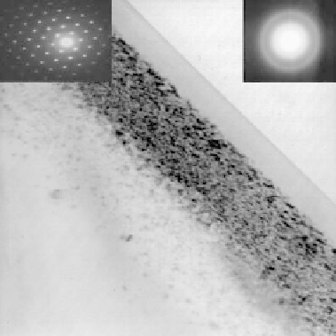
The cross-sectional transmission electron microscopy (TEM) micrograph of the hydrogen-
implanted silicon wafer in Figure 19.9 reveals the formation of defects. There exists a top amor-
phous zone (about 60 nm in thickness) and a dense dislocation zone (about 150 nm). The dense
dislocation zone is located around the projected range of H
+
. Figure 19.10 plots the atomic disloca-
tion density versus depth derived from channeling-RBS (c-RBS) and the hydrogen elemental depth
profi le acquired by secondary ion mass spectrometry (SIMS). Hydrogen is mainly found on the
near-surface to about 170 nm (
8 at.%), which is the projected range of H
+
obtained from the SRIM
code. A total atomic displacement zone (amorphous silicon a-Si) is extended from the top surface to
the depth of about 50 nm (slightly different from the TEM results due to calibration and instrumen-
tation issues) followed by a dislocation zone located close to the projected range of H
+
. Hence, the
implanted sample consists of a highly hydrogen-doped surface with high crystalline disorder.
∼
TABLE 19.1
Implantation Parameters
Implantation voltage (kV)
30
Pulse frequency (Hz)
50
Pulse duration (s)
500
RF discharge power (W)
1400
Implantation time (min)
20
∼
1.4
×
10
17
Implantation dose/cm
2
60 nm
150 nm
FIGURE 19.9
Cross-sectional views of hydrogen-implanted silicon wafer obtained from TEM analysis.
(From Liu, X.Y. et al.,
Biomaterials
, 25, 5575, 2004. With permission.)