Biomedical Engineering Reference
In-Depth Information
s
!
þ
tan
Ł
o
r
c
¼
r
cos
Ł
o
þ
cos
2
Ł
o
þ
(1
þ
sin
Ł
o
)
1
þ
tan
2
Ł
o
cos
Ł
o
ð
2
:
10
Þ
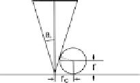
Fig. 2.31. Simplified view of probe deconvolution. If the cross-section of the probe geometry is
described as an upside down triangle, it is simple to remove the effect of the probe from an image of a
nanoparticle. The actual diameter of the nanoparticle is calculated using the equation at the right.
However, real probes do not have the shape of an upside down triangle.
the probe incorrectly before it is placed in the microscope can also cause probe damage.
For example, if the probe is exposed to high electric fields, the probe tip can be blown off
by electrostatic discharge. Finally, the probe tip can get dirty from the packing materials
used to hold the probe while shipping.
2.5.4 Probe shape deconvolution
If the probe geometry is analytically known, it is possible to remove the probe geometry's
effect on an AFM image by a process called deconvolution (see Figure 2.31 for a two-
dimensional representation of the problem). Unfortunately the geometry of AFM probes is
not well known from first principles, as they do not normally have simple geometrical
shapes. Furthermore, because the method of manufacturing such probes is not perfectly
reproducible, there will be variability from batch to batch and even considerable variation
in probe characteristics produced on the same silicon wafer. Thus, in order to correctly
deconvolve the tip contributions from an image, it is necessary to characterize each tip on
a case by case basis.
Unfortunately, it is difficult to find a technique to accurately and non-destructively
measure the tip geometry. Both TEM and SEM have been tried [45-47], but although
either technique could have in principle sufficient resolution for the task, there are a
number of difficulties. Neither technique gives real three-dimensional information, so
superposition of various rotated images is necessary to fully characterize the probe. The
resolution required must be similar to that of the details in the image, i.e. the same as the
resolution of AFM. To achieve such resolutions, electron microscopes must be operated at
high driving voltages, and with such high voltages sharp features such as the probe are
easily damaged by over-charging, especially without metal coating, which can alter the
profile of the tip. Such difficulties mean that these techniques are quite impractical. The
ideal instrument to get three-dimensional, high-resolution measurements of the probe is
the AFM itself. This can be used by tip self-imaging which is done by using the AFM to
image a spike-like feature (see for example the tip-characterization samples described in
Appendix A). This results in the spike imaging the tip, i.e. the resulting image is an image
of the tip, only somewhat dilated by the sample, assuming that the radius of the spike is
much less than that of the tip. A related technique is to image a very well-known sample
such as well-characterized nanoparticles [48, 49]. Knowing the correct sample geometry
the dilation by the tip is easy to extract. These techniques are somewhat more convenient