Biomedical Engineering Reference
In-Depth Information
9 nm
17 nm
FFT
0 nm
0 nm
0 nm
9 nm
0 nm
17 nm
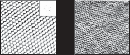
Fig. 7.5. Two examples of atomic lattice resolution. Left: muscovite mica (inset shows the Fourier
transform image). Right: self-assembled monolayer on Au (111) surface. These images are not true
atomic resolution as no dislocations, point defects or extra surface atoms were seen [372]. Repro-
duced with permission from [426] and [427].
Images such as those presented in Figure 7.5 allow us to visualize the atomic lattice of
crystalline materials, and to make some measurements of it, but their use is limited. The
ability to obtain true atomic resolution, and apply it to imperfect or mixed systems is
much more useful. This can be achieved under UHV conditions [428] (usually though not
always in non-contact FM-AFM), and also in liquid [372, 429, 430]. For instance, this
technique allows researchers to observe the atomic structure of a large number of metals,
semiconductors, metal oxides [26, 431, 432], and of different materials deposited on top of
one another [425, 433]. Crucially, with true atomic resolution, all this is possible with
(limited) mixing of components, and allows researchers to image holes, dislocations,
stacking faults, sub-monolayers, etc. [372, 434], see Figure 7.6 for examples. This tech-
nique can even reveal sub-atomic detail, e.g. information of molecular orbitals can be
determined in some cases [435].
True atomic resolution is more routinely achieved in STM than AFM [434]. The main reason
for this is that in the imaging mechanism of STM, only the atom on the tip which is the closest to
the sample will interact via tunnelling. This means that by manufacturing a 'rough' tip, an
atomically sharp probe can be produced. Such an approach does not work for AFM, because
even with a very sharp probe, the less specific nature of the interaction means that atoms much
further away from the surface than the last one on the tip will also interact with the surface.
However, the highly specific nature of the interaction of STM probes with the surface can give
rise to some surprising results. For example, because the STM probes the electron density in the
surface orbitals, changing the sample bias can make some atoms appear to appear and disappear
[436]. A further example is the case of graphite (usually in the form of HOPG). For many years,
achieving atomic resolution on graphite has been used as a quality test for both STM and AFM
instruments, and it is a very widely studied material by both techniques [428, 437-439]. Some
early STM studies appeared to show the expected hexagonal rings of graphite in STM images,
but these were later shown to be artefacts caused by double tips [440]. Although in two
dimensions, it would appear that all the atoms are equivalent, consideration of the three-
dimensional structure of graphite shows that three of the atoms are in one form, named
Æ
,
and three are in another form, termed
atoms have lower electron density a the surface,
and therefore are invisible to STM [441]. Changing the sample bias does not change this. Work
by Hembacher
et al
. was able to show that the 'missing' atoms could be seen by AFM [428].
.The
Æ