Biomedical Engineering Reference
In-Depth Information
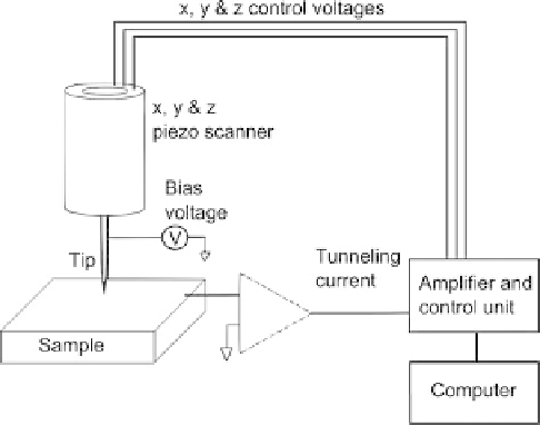
Fig. 1.3. Simplified schematic of a scanning tunnelling microscope (STM).
raster pattern. Like the topografiner, the movement of the tip over the surface in
x
,
y
and
z
is controlled with three piezoelectric elements (in Figure 1.3, the three elements are
integrated together in a tube structure; this is discussed further in Chapter 2). The distance
the
z
piezo has to move up and down to maintain the tunneling current at the same value is
equivalent to the sample height, so the computer can build up a map of sample height as
the tip scans over the surface. The reason the instrument was so much more successful than
the topografiner is that electron tunnelling is much more sensitive to tip-sample distance
than field emissions, so the probe could be scanned very close to the surface. In fact, the
probability of electron tunnelling is so strongly dependent on distance that effectively only
the very last atom of the STM tip can undergo tunnelling. Because it is this last atom which
is most sensitive to tunnelling from the surface, the structure of the tip far from the surface
is not very important, so atomically sharp tips are easy to produce. For their very first
experiments, Binnig and Rohrer levitated the entire instrument magnetically to counter
vibrations; however later designs did not require this. The results of these early experi-
ments were astounding; Binnig and Rohrer were able to see individual silicon atoms on a
surface, [14, 16]. Without the STM, attaining this kind of resolution required a transmis-
sion electron microscope (TEM), which weighs thousands of kilograms, and fills a room.
Furthermore, when the STM was invented, atomic structure could only be observed
indirectly by diffraction patterns, while the STM could do it directly by imaging individual
atoms. That the STM could do this when it was only a small instrument, suspended with
springs to counter vibrations, seemed incredible, and Binnig and Rohrer later shared the
Nobel Prize for physics in 1986 for the invention of the STM [17].
Although the STM was considered a fundamental advancement for scientific research, it
had limited applications, because it worked only on electrically conductive samples.
Despite these limits, STM remains a very useful technique, and is used widely in particular
in physics and materials science to characterize the atomic structure of metals and semi-
conductors, and for fundamental studies of electronic effects at metal surfaces. Figure 1.4
shows an STM image, illustrating the atomic resolution routinely obtained in STM.