Environmental Engineering Reference
In-Depth Information
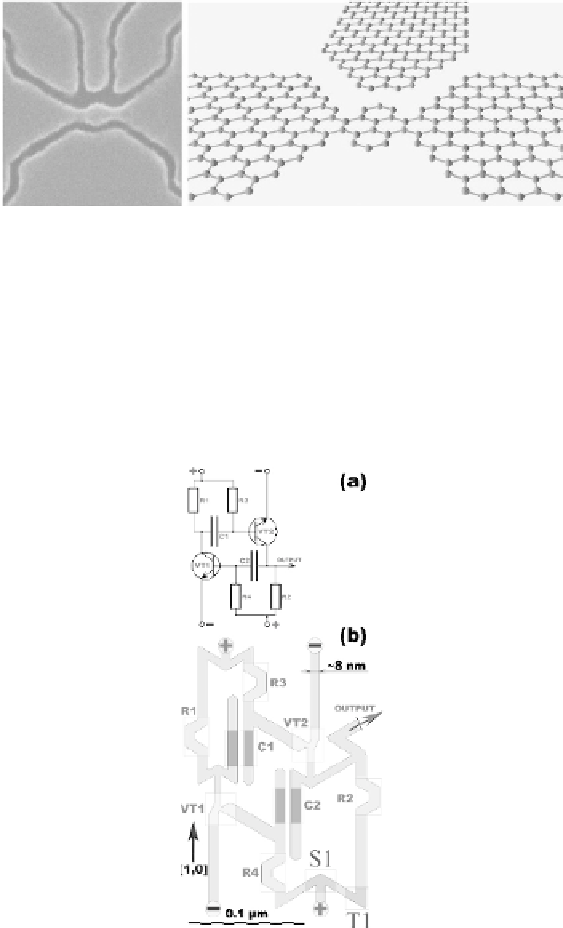
Figure 3.13
Graphene devices. (Left) Scanning electron micrograph of a
graphene-based single-electron transistor. The dark areas are gaps in the
photoresist mask where graphene is removed by plasma etching. The small
quantum dot in the center is connected to contact regions through narrow
constrictions, and there are four side gates. (Right) Schematic showing a
hypotheticalgraphene-basedsingle-electrontransistorbasedonaquantum
dot that contains only a few benzene rings. Reprinted from Ref. [54] with
kind permission from Prof. Sir Andre Konstantin Geim, University of
Manchester, UK.
Figure 3.14
(a) Flip-flop circuit without wire crossings. (b) Its possible
GNR-based counterpart patterned from a single graphene sheet. To keep
this drawing compact, the capacitors C1 and C2 are not drawn to scale.
Reprinted with permission from Ref. [55]. Copyright 2007 American
Chemical Society.